Method and node device for constructing data center switching network

A switching network and data center technology, applied in the direction of data exchange through path configuration, electromagnetic network arrangement, etc., can solve the problems of delay deterioration, chip energy consumption increase, switching network growth, etc., to achieve high interconnection bandwidth and average delay , the effect of simple wiring

Active Publication Date: 2017-05-10
BEIJING UNIV OF POSTS & TELECOMM
View PDF8 Cites 0 Cited by
  • Summary
  • Abstract
  • Description
  • Claims
  • Application Information

AI Technical Summary

Problems solved by technology

[0008] In terms of data exchange delay, since the interconnection between servers far away in the tree network structure must go through many hops, the store-and-forward process of each hop introduces a certain delay, and this delay occurs when the network is congested. It will worsen, resulting in uncontrollable end-to-end delay on the whole, which greatly affects the performance of upper-layer applications
[0009] In terms of energy consumption, the greater the number of ports supported by electrical switching equipment and the higher the processing speed, the overall energy consumption of the switching network will increase correspondingly super-linearly, because not only the energy consumption of the chip itself increases, but also the ventilation and heat dissipation are improved. and cooling energy consumption

Method used


Image

  • Method and node device for constructing data center switching network
  • Method and node device for constructing data center switching network
  • Method and node device for constructing data center switching network

Examples


Embodiment 1

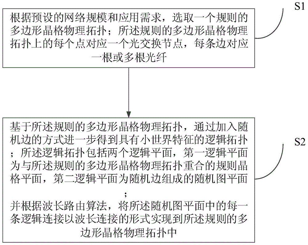
[0048] Such as image 3 As shown, the embodiment of the present invention provides a method for constructing a data center switching network, including:

[0049] S1. According to the preset network scale and application requirements, select a regular polygonal lattice physical topology; each point on the regular polygonal lattice physical topology corresponds to an optical switching node, and each edge corresponds to one or more root fiber;

[0050] S2. Based on the regular polygonal lattice physical topology, a logical topology with small-world characteristics is further obtained by adding random edges; the logical topology includes two logical planes, the first logical plane is a polygon with the regular A regular lattice plane where the physical topology of the lattice coincides, and the second logical plane is a random graph plane composed of random edges;

[0051] And according to the wavelength routing algorithm, implement each logical connection in the random graph pl...

Embodiment 2

[0071] Such as Figure 5 As shown, the embodiment of the present invention also provides a node device for constructing a data center switching network, and the node device includes several demultiplexing modules, a random graph plane optical switching processing module, a regular lattice plane optical switching processing module, several a multiplexing module, and an electrical packet switching module;

[0072] Wherein, the optical fiber is decomposed into multiple wavelengths after passing through the demultiplexing module, and a part of the wavelengths is input to the random graph plane optical switching processing module, and then output to the multiplexing module after being processed by adding and dropping; the other part of the wavelengths is input to the regular lattice plane optical switching processing module, and output to the multiplexing module after being processed by adding and dropping;

[0073] The electrical packet switching module implements electrical doma...

Embodiment 3

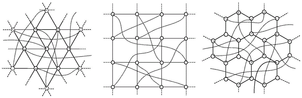
[0081] The present invention is described below by specific embodiment:

[0082] Such as Image 6 As shown, taking the physical topology of a hexagonal lattice as an example, each solid line in the figure represents an optical fiber, and each point represents a node device described in the present invention. The signal transmission in the optical fiber is unidirectional. To simplify the discussion, it is assumed that there are at least three available wavelengths, namely λ1, λ2 and λ3. Among them, λ1 is used to provide a ring data bus in each cell, and each cell can be regarded as an independent optical burst switching ring network. λ2 and λ3 belong to the wavelength resources used to build the topological plane of the random graph. Here, the two wavelength connections of λ2 and λ3 are bidirectional. This is to ensure that the data round-trip and return delays are as consistent as possible when two nodes that are far away are interconnected through a random graph plane.

[...


PUM


Abstract

The invention relates to the network and optical switching technical field and provides a method of constructing a data center switching network and a node apparatus. The method comprises the step S1 of selecting a regular polygonal crystal lattice physical topology according to a preset network scale and application demands. Each dot in the regular polygonal crystal lattice physical topology is corresponding to one optical switching node. Each side is corresponding to one or more fibers. The method further comprises the step S2 of acquiring a logical topology complying with small-world network characteristics in line with the application demands according to the regular polygonal crystal lattice physical topology. The logical topology comprises two logical planes. The first logical plane is a regular crystal plane. The second logical plane is a random graph plane composed of random sides. A data center inner switching network constructed through the method achieves any large-scale port number, random expansion and simple wiring. While the method makes a large scale and flexible expansion achieved, the method further guarantees a relatively high Internet bandwidth and a relatively low average time delay between any two servers.

Description

technical field [0001] The invention relates to the technical field of network and optical switching, in particular to a method and a node device for constructing a data center switching network. Background technique [0002] The main task of the switching network in the data center is to provide arbitrary interconnection between thousands of servers. The primary feature of this kind of network is that the port scale is huge, usually on the order of thousands or even hundreds of thousands; secondly, it requires high throughput and the lowest possible end-to-end delay; in addition, it needs to have good scalability, so that Support the expansion requirements of higher speed and larger port size in the future. [0003] In order to build such a data communication network, the current most common way is to cascade packet switching devices to form a multi-layer tree structure. Such as figure 1 As shown, the ToR switch (Top of RackSwitch) is directly connected to a server in a ...

Claims


Application Information

Patent Timeline
Patent Type & Authority Patents(China)
IPC IPC(8): H04B10/27H04L12/28
Inventor 郭宏翔伍剑张东旭
Owner BEIJING UNIV OF POSTS & TELECOMM
Why Eureka
Try Eureka