Deep trench isolated anti-crosstalk photoelectric detector and manufacturing method thereof

A photodetector, anti-crosstalk technology, applied in semiconductor/solid-state device manufacturing, circuits, electrical components, etc., can solve the problems of poor resistance-capacitance characteristics, loss of light energy, reduced photodetector responsivity, etc., to reduce the capacitance area. Small, improve the response speed, reduce the effect of intrinsic dark current

Active Publication Date: 2015-09-09
CHONGQING EAGLE VALLEY OPTOELECTRONICS
View PDF6 Cites 2 Cited by
  • Summary
  • Abstract
  • Description
  • Claims
  • Application Information

AI Technical Summary

Problems solved by technology

[0003] In order to reduce the impact of photoelectric crosstalk, most of the existing quadrant photodetector chips use PN junctions to isolate each quadrant. PN junctions are used as electrical isolation. For near-infrared wavelengths (1064nm), a high withstand voltage is generally required. Therefore, the depletion region must be Wide, but this will produce bad resistance and capacitance characteristics; another method is to increase the area of ​​the blind zone, which can not only improve the withstand voltage, but also reduce the crosstalk between quadrants, but the increase of the blind zone will lose more light energy. At the same time, There are also strict requirements on the size of the blind area during the use of the device; another method is to thin the photo-generated carrier generation area, although it can also reduce the photoelectric crosstalk, but thinning the thickness of the photo-generated carrier generation area Infrared 1064nm wavelength, the light absorption thickness will be reduced accordingly, which will seriously reduce the responsivity of the photodetector

Method used


Image

  • Deep trench isolated anti-crosstalk photoelectric detector and manufacturing method thereof
  • Deep trench isolated anti-crosstalk photoelectric detector and manufacturing method thereof
  • Deep trench isolated anti-crosstalk photoelectric detector and manufacturing method thereof

Examples


Embodiment Construction

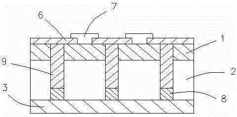
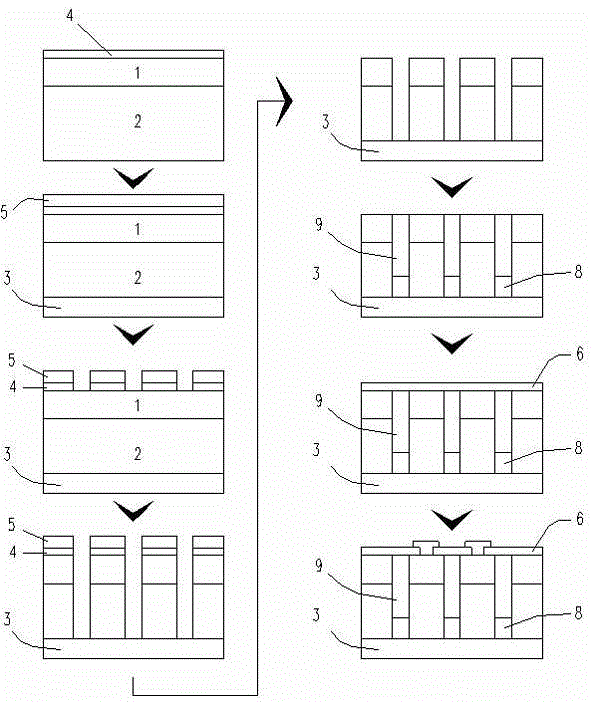
[0023] A deep groove isolation anti-crosstalk photodetector, comprising a P-i-N layered structure sequentially stacked by a P-type diffusion layer 1, a substrate layer 2 and an N-type diffusion layer 3, and an isolation region is arranged on the P-i-N layered structure , the isolation region divides the photosensitive surface of the P-i-N layered structure into multiple quadrants, and its innovation is that the isolation region is realized by the following structure: a deep groove is made on the photosensitive surface of the P-i-N layered structure, and the cross-section of the deep groove The contour matches the outer contours of multiple quadrants, the axial direction of the deep groove is the same as the stacking direction of the P-i-N layered structure, the depth of the deep groove reaches the upper end surface of the N-type diffusion layer 3, and the deep groove is filled with an insulating substance.

[0024] Further, the insulating material adopts spin-on glass and polyi...


PUM


Abstract

The invention discloses a deep trench isolated anti-crosstalk photoelectric detector, comprising a P-i-N laminar structure formed by sequentially laminating a P-type diffusion layer, a substrate layer and an N-type diffusion layer, wherein an isolation region is formed on the P-i-N laminar structure and divides the photo-surface of the P-i-N laminar structure into a plurality of quadrants. The photoelectric detector is characterized in that the isolation region is realized by adopting the following structure: a deep trench is made in the photo-surface of the P-i-N laminar structure, the cross section contour of the deep trench is matched with the outer contours of the plurality of quadrants, the axial direction of the deep trench is the same as the laminating direction of the P-i-N laminar structure, the depth of the deep trench reaches the upper end surface of the N-type diffusion layer, and the deep trench is filled with an insulating material. The photoelectric detector has the advantages: each quadrant of the quadrant photoelectric detector is effectively isolated, the area of the depletion layer of the photoelectric detector is reduced, the internal junction capacitance area is reduced, the RC time constant is reduced, and the response speed of a device is improved; and the deep trench is positioned in the body of the quadrant photoelectric detector, so that the influence of surface defects on the device is avoided.

Description

technical field [0001] The invention relates to a photodetector manufacturing technology, in particular to a photodetector with deep groove isolation and anti-crosstalk and a manufacturing method thereof. Background technique [0002] In the prior art, an isolation region (also called a blind region) is generally made on a semiconductor silicon detector to form a quadrant photodetector. When the quadrant photodetector is working, photogenerated carriers are generated under the action of light. Under the action of electric field, orderly and directional movement is made to form photocurrent, so that each quadrant outputs signals independently. Due to the disordered movement of some photogenerated carriers in the generation region and the transition region, the photogenerated carriers will enter the surrounding photosensitive regions from their own photosensitive regions, thereby forming photoelectric crosstalk. ), silicon quadrant photodetectors that require a thick depl...

Claims


Application Information

Patent Timeline
Patent Type & Authority Applications(China)
IPC IPC(8): H01L27/146H01L21/762
Inventor 唐政维刘新勾伯桐王康林林灵彭虎刘建文
Owner CHONGQING EAGLE VALLEY OPTOELECTRONICS
Why Eureka
Try Eureka