

A Control Method for Realizing Low Voltage Switch Stress
A control method and switching stress technology, applied in control/regulating systems, electrical components, regulating electrical variables, etc., can solve the problems of reduced energy conversion efficiency, high voltage stress of switching devices, electromagnetic interference, etc., to reduce conduction losses and switching losses, improve operating efficiency, and reduce voltage stress
- Summary
- Abstract
- Description
- Claims
- Application Information
AI Technical Summary
Problems solved by technology
Method used
Image

Examples
Embodiment Construction
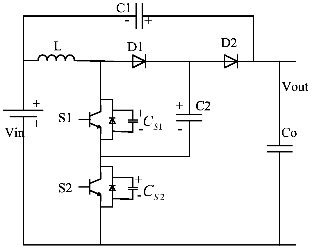
[0029] Depend on image 3 It can be seen that the low voltage switching stress booster circuit of the present invention includes input voltage Vin, switching elements S1, S2, diodes D1, D2, inductor L, input capacitor C1, intermediate capacitor C2 and output capacitor Co. Due to the characteristics of switching devices, switching elements S1 and S2 respectively have parasitic capacitance C S1 、C S2 .
[0030] combined with image 3The structure of the present invention is described in detail. The specific connection relationship is as follows: the positive pole of the input voltage Vin is connected to one end of the inductance L and the negative end of the input capacitor C1, and the other end of the inductance L is connected to the collector of the switching element S1 and the anode of the diode D1. The emitter of the switching element S1 is connected to the collector of the switching element S2, the emitter of the switching element S2 is connected to the negative pole of ...
PUM
 Abstract
Description
Claims
Application Information