A Photonic Crystal Optical Bridge with High Transmission Rate, High Return Loss and High Isolation

A high return loss, photonic crystal technology, applied in the direction of optical waveguide light guide, optics, light guide, etc., can solve the problems of large volume and inability to integrate with optical path, and achieve the effect of small structure volume, high extinction ratio and easy integration

Inactive Publication Date: 2018-06-05
欧阳征标 +1
View PDF4 Cites 0 Cited by
  • Summary
  • Abstract
  • Description
  • Claims
  • Application Information

AI Technical Summary

Problems solved by technology

[0002] Traditional optical bridges apply the principle of geometric optics, so they are relatively large in size and cannot be used in optical path integration

Method used


Image

  • A Photonic Crystal Optical Bridge with High Transmission Rate, High Return Loss and High Isolation
  • A Photonic Crystal Optical Bridge with High Transmission Rate, High Return Loss and High Isolation
  • A Photonic Crystal Optical Bridge with High Transmission Rate, High Return Loss and High Isolation

Examples


Embodiment 1

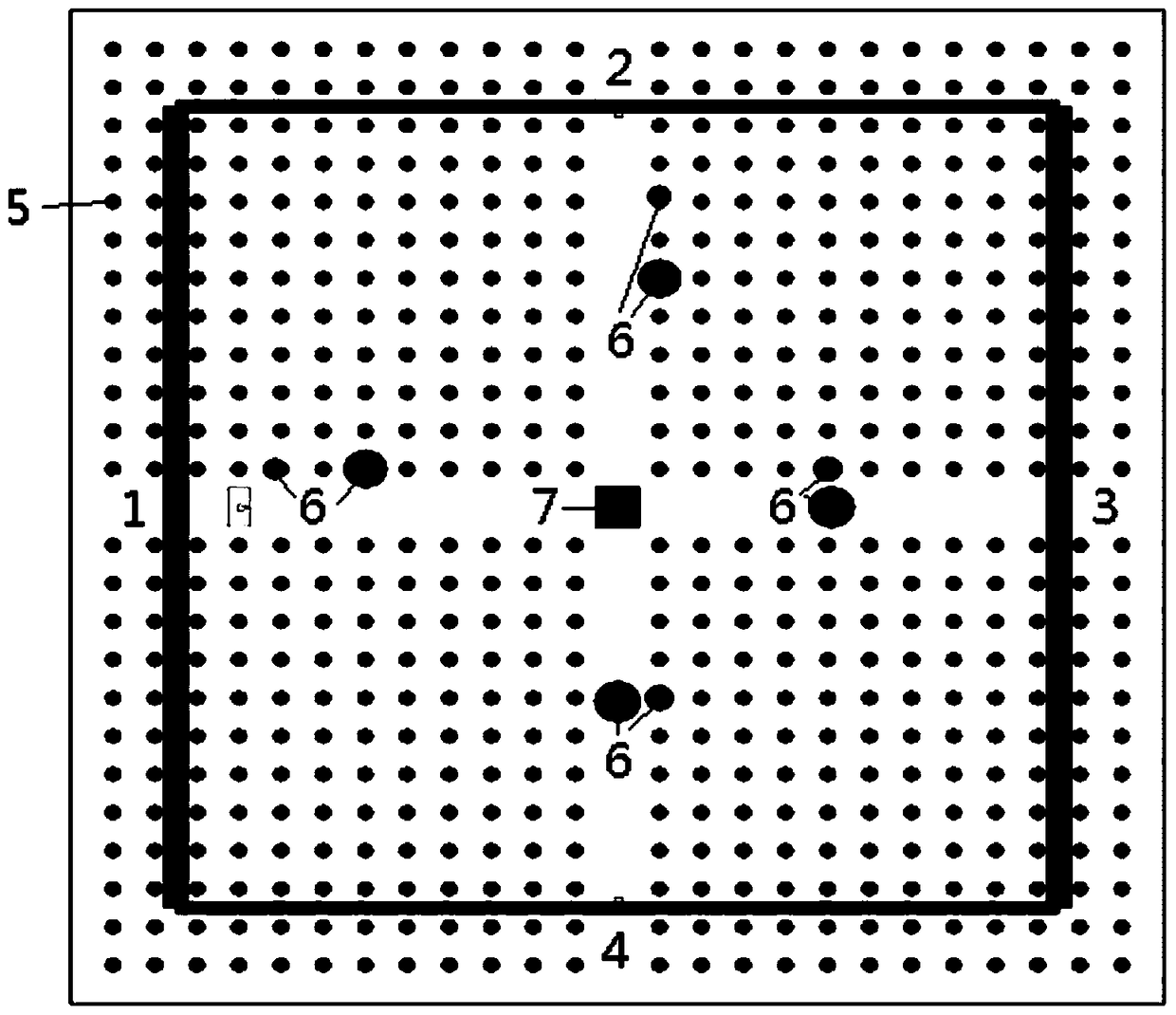
[0038]Taking the incident wavelength λ=1.500000 (μm), a=0.504000 (μm), the diameter of the high refractive index background medium column at this time is 0.090720 (μm), and the diameter R11 of the two circular point defects at the input end 1 of the optical signal A and R12 are 0.251601 (μm) and 0.135483 (μm), respectively, and the positions are (-5.800270, 0.974726) (μm) and (-7.883409, 0.967054) (μm); two circular point defects at the input terminal 2 of the optical signal B The diameters R21 and R22 are 0.270967 (μm) and 0.164523 (μm) respectively, and the positions are (4.930629, 0.001354) (μm) and (4.838283, 0.967705) (μm); two circular points at the output end 3 of the optical signal A The diameters R31 and R32 of the defect are 0.251601 (μm) and 0.135483 (μm) respectively, and the positions are (0.974726, 5.800270) (μm) and (0.967054, 7.883409) (μm); The diameters R41 and R42 of point defects are 0.270967 (μm) and 0.164523 (μm), respectively, and the positions are (0.00...

Embodiment 2

[0040] Taking the incident wavelength λ=1.550000 (μm), a=0.520800 (μm), the diameter of the high refractive index background medium column at this time is 0.093744 (μm), and the diameter of two circular point defects 6 at the input end 1 of the optical signal A R11 and R12 are 0.259988 (μm) and 0.140000 (μm) respectively, and the positions are (-5.993548, 1.007217) (μm) and (-8.146190, 0.999290) (μm); two circular points at the input terminal 2 of optical signal B The diameters R21 and R22 of the defect are 0.280000 (μm) and 0.170008 (μm) respectively, and the positions are (5.094984, 0.001400) (μm) and (4.999560, 0.999962) (μm); The diameters R31 and R32 of the point defects are 0.259988 (μm) and 0.140000 (μm) respectively, and the positions are (1.007217, 5.993548) (μm) and (0.999290, 8.146190) (μm); two circles at the output terminal 4 of the optical signal B The diameters R41 and R42 of the point defects are 0.280000 (μm) and 0.170008 (μm) respectively, and the positions a...

Embodiment 3

[0042] Taking the incident wavelength λ=1.600000 (μm), a=0.537600 (μm), the diameter of the high refractive index background medium column at this time is 0.096768 (μm), and the diameter R11 of the two circular point defects at the input end 1 of the optical signal A and R12 are 0.268374 (μm) and 0.144516 (μm), respectively, and the positions are (-6.186888, 1.039707) (μm) and (-8.408970, 1.031525) (μm); two circular point defects at the input terminal 2 of the optical signal B The diameters R21 and R22 are 0.289032 (μm) and 0.175492 (μm) respectively, and the positions are (5.259338, 0.001445) (μm) and (5.160836, 1.032218) (μm); two circular points at the output end 3 of the optical signal A The diameters of defects R31 and R32 are 0.268374 (μm) and 0.144516 (μm) respectively, and the positions are (1.039707, 6.186888) (μm) and (1.031525, 8.408970) (μm); The diameters R41 and R42 of point defects are 0.289032 (μm) and 0.175492 (μm), respectively, and the positions are (0.0014...


PUM


Abstract

The invention discloses a photonic crystal light bridge with high transmission rate, high return loss and high isolation, aiming to provide a photon crystal light bridge with high transmission rate, high return loss, easy integration and high efficiency. It includes a photonic crystal with a forbidden band and a photonic crystal waveguide, as well as two input terminals and two output terminals. The left, upper, right and lower sides of the photonic crystal waveguide are respectively two input terminals and two output terminals. ; The photonic crystal waveguide is composed of a photonic crystal vertical waveguide and a photonic crystal horizontal waveguide in a cross shape in the middle; a waveguide defect dielectric column is set in the photonic crystal cross waveguide; two circular defect dielectric columns are respectively set in the four ports of the photonic crystal waveguide , the square defect dielectric column is located in the center of the junction between the vertical waveguide and the horizontal waveguide; the two input ends of the photonic crystal waveguide input two beams of optical signals respectively, and form a cross of optical paths in the common central area to perform mutual non-interference transmission. Output from different ports in a straight line direction.

Description

technical field [0001] The invention relates to the field of tiny optical optical bridges, in particular to a photonic crystal optical bridge with high transmission rate, high return loss and high isolation based on photonic crystal technology. Background technique [0002] Traditional optical bridges apply the principle of geometric optics, so they are relatively large in size and cannot be used in optical path integration. Based on photonic crystals, tiny devices can be fabricated, including photonic crystal light bridges. The photonic crystal waveguiding optical path of the optical bridge is generally constructed by introducing line defects into the photonic crystal with complete band gap. We introduce the multiple scattering method: one or more point defects are introduced into the line defects that make up the optical bridge, and they are used as scatterers to generate scattered waves that can cancel the reflected waves propagating in the device, and the positions of t...

Claims


Application Information

Patent Timeline
Patent Type & Authority Patents(China)
IPC IPC(8): G02B6/10G02B6/122
Inventor 欧阳征标黄浩
Owner 欧阳征标
Why Eureka
Try Eureka