Liquid crystal display panel and manufacturing method thereof

A technology for a liquid crystal display panel and a manufacturing method, which is applied in semiconductor/solid-state device manufacturing, optics, instruments, etc., can solve problems such as cost reduction and high cost, and achieve the effect of saving photosensitive spacer processes.

Active Publication Date: 2015-09-23
WUHAN CHINA STAR OPTOELECTRONICS TECH CO LTD
View PDF7 Cites 11 Cited by
  • Summary
  • Abstract
  • Description
  • Claims
  • Application Information

AI Technical Summary

Problems solved by technology

[0004] However, the production of photosensitive spacers on the color filter substrate requires an additional high-cost photolithography process compared to the traditional color filter substrate, which is not conducive to cost reduction.

Method used


Image

  • Liquid crystal display panel and manufacturing method thereof
  • Liquid crystal display panel and manufacturing method thereof
  • Liquid crystal display panel and manufacturing method thereof

Examples


Embodiment Construction

[0023] The following descriptions of the various embodiments refer to the accompanying drawings to illustrate specific embodiments in which the present invention can be practiced.

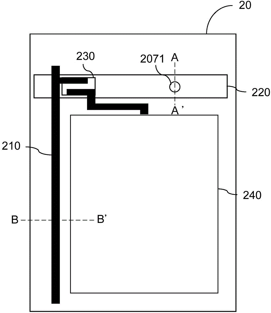
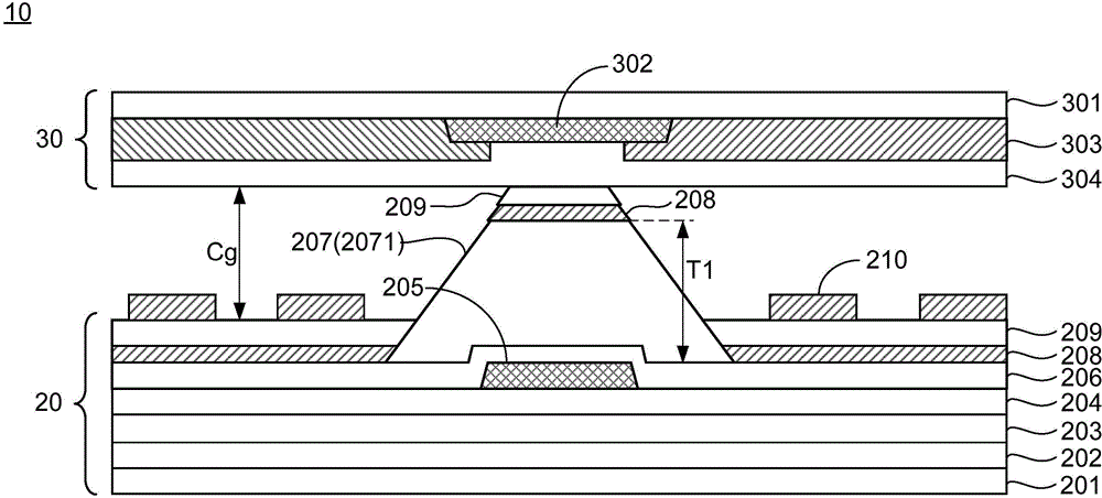
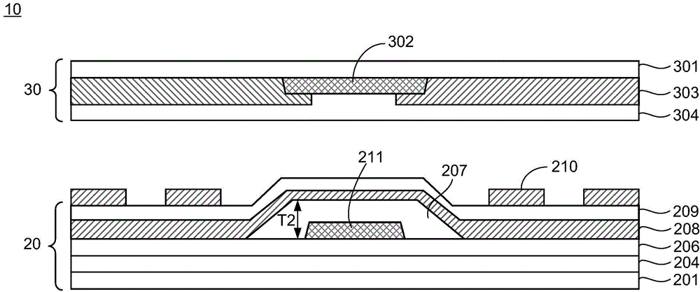
[0024] refer to Figure 1 to Figure 3 , figure 1 It is a schematic plan view of the array substrate of the liquid crystal display panel of the present invention, figure 2 for figure 1 The cross-sectional schematic diagram of the liquid crystal display panel on the line AA', image 3 for figure 1 The schematic cross-sectional view of the liquid crystal display panel on the BB' line segment. As shown in the figure, the liquid crystal display panel 10 of this embodiment includes an array substrate 20 , a color filter substrate 30 and a liquid crystal layer (not shown) therebetween.

[0025] like figure 1 as shown, figure 1 A pixel structure on the array substrate 20 is shown. The array substrate 20 includes data lines 210, scanning lines 220 and thin film transistors 230. The data lines 210 an...


PUM

PropertyMeasurementUnit
thicknessaaaaaaaaaa

Abstract

The invention provides a liquid crystal display panel and a manufacturing method thereof. The liquid crystal display panel comprises an array substrate and a color film substrate. The array substrate comprises a data line, a scanning line, a thin film transistor and an open region. The array substrate further comprises a patterned flat layer formed on the data line, the scanning line and the thin film transistor and exposed out of the open region. A columnar protrusion is formed at the portion, located on the scanning line, of the patterned flat layer, the columnar protrusion is supported between the array substrate and the color film substrate, no spacer needs to be additionally manufactured, and therefore the procedure of manufacturing photosensitive spacers on the color film substrate is omitted.

Description

【Technical field】 [0001] The invention relates to the field of liquid crystal display, in particular to a liquid crystal display panel and a method for manufacturing the liquid crystal display panel. 【Background technique】 [0002] A traditional liquid crystal display panel includes a color filter (CF, Color filter) substrate, an array substrate and a liquid crystal. The color filter substrate includes a first glass substrate, a black matrix (BM, Black Matrix) layer, a colored pattern layer and a protective layer (OC, Over Coat) layer, the first glass substrate, a black matrix layer, a colored pattern layer and a protective layer The array substrate is sequentially stacked and arranged as a whole; the array substrate includes a second glass substrate, a gate line layer, an insulating layer, a semiconductor layer, a metal layer and a passivation layer, and the second glass substrate, a gate line layer, an insulating layer, a semiconductor layer, a metal layer The passivation...

Claims


Application Information

Patent Timeline
Patent Type & Authority Applications(China)
IPC IPC(8): G02F1/1339H01L21/77
CPCG02F1/1339H01L21/77G02F1/13394H01L27/1288
Inventor 陈彩琴
Owner WUHAN CHINA STAR OPTOELECTRONICS TECH CO LTD
Why Eureka
Try Eureka