
Copper foil with carrier, printed wiring board, laminate, electronic machine and method for manufacturing printed wiring board

A technology for printed wiring boards and manufacturing methods, applied in printed circuit parts, chemical instruments and methods, secondary processing of printed circuits, etc., can solve problems such as residues and poor insulation of circuit patterns, and achieve the effect of good circuit formability

Active Publication Date: 2015-09-30
JX NIPPON MINING & METALS CO LTD
View PDF52 Cites 8 Cited by
  • Summary
  • Abstract
  • Description
  • Claims
  • Application Information

AI Technical Summary

Problems solved by technology

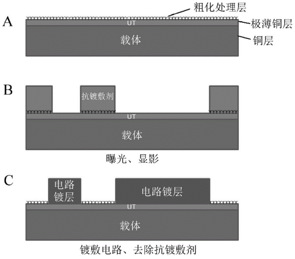
[0005] However, if such an ultra-thin copper layer with a large outline (concave-convex, roughness) is used on a printed wiring board, especially a semiconductor package substrate that must form a fine circuit pattern, unnecessary copper particles will remain during circuit etching, resulting in Problems such as poor insulation between circuit patterns

Method used


Image

  • Copper foil with carrier, printed wiring board, laminate, electronic machine and method for manufacturing printed wiring board
  • Copper foil with carrier, printed wiring board, laminate, electronic machine and method for manufacturing printed wiring board
  • Copper foil with carrier, printed wiring board, laminate, electronic machine and method for manufacturing printed wiring board

Examples


Embodiment

[0331] Hereinafter, it demonstrates based on an Example and a comparative example. In addition, this Example is just an example, and is not limited to this example.

[0332] 1. Manufacture of copper foil with carrier

[0333] As a copper foil carrier, a 35-micrometer-thick long electrolytic copper foil (JTC manufactured by JX Nippon Oil Metal Co., Ltd.) and a 33-micrometer-thick rolled copper foil (C1100 manufactured by JX Nikko Nippon Oil Metal Co., Ltd.) were prepared. The glossy side (bright side) of the copper foil is subjected to nickel (Ni) or cobalt (Co) plating as metal plating using a roll-to-roll continuous plating line under the following conditions, followed by BTA treatment as chromate treatment or treatment with organic matter, thereby forming the intermediate layer. In addition, "degreasing" and "pickling" in Table 1 represent the pretreatment of performing nickel (Ni) plating on the surface of the carrier to be nickel-plated or cobalt-plated under the followi...


PUM

PropertyMeasurementUnit
Thicknessaaaaaaaaaa

Abstract

The invention discloses a copper foil with a carrier, a printed wiring board, a laminate, an electronic machine and a method for manufacturing the printed wiring board. Specifically, the invention provides a copper foil with a carrier, and the copper foil has good circuit formability. The copper foil with the carrier sequentially has a carrier, an intermediate layer and an extremely thin copper layer, and when the copper foil with the carrier is heated at a speed of 30 DEG C / min to 500 DEG C, the water content that is less than generated is 160ppm / g.

Description

technical field [0001] The present invention relates to a copper foil with a carrier, a printed wiring board, a laminate, an electronic device, and a method for manufacturing the printed wiring board. Background technique [0002] Printed wiring boards are generally manufactured through the steps of bonding an insulating substrate to copper foil to form a copper-clad laminate, and then forming a conductive pattern on the surface of the copper foil by etching. With the increasing demand for miniaturization and high performance of electronic equipment in recent years, high-density mounting of mounted parts or high frequency of signals has continued to develop, and printed wiring boards are required to miniaturize (fine-pitch) or respond to conductor patterns. high frequency etc. [0003] Corresponding to fine-pitching, copper foil with a thickness of 9 μm or less, and furthermore, a thickness of 5 μm or less has recently been demanded. However, such extremely thin copper foil...

Claims


Application Information

Patent Timeline
IPC IPC(8): B32B15/01B32B15/20H05K1/09H05K3/28
Inventor 宫本宣明本多美里石井雅史
Owner JX NIPPON MINING & METALS CO LTD
Learn More