Transparent conductive film and capacitive touch screen including it
A technology of transparent conductive film and transparent substrate, applied in the direction of electrical digital data processing, input/output process of data processing, instruments, etc., can solve the problems of poor anti-fouling and slip resistance of transparent conductive film, obvious three-dimensional lines, etc., and achieve stress difference The effect of reducing, simplifying the preparation process and avoiding pollution
- Summary
- Abstract
- Description
- Claims
- Application Information
AI Technical Summary
Problems solved by technology
Method used
Image
Examples
Embodiment 1
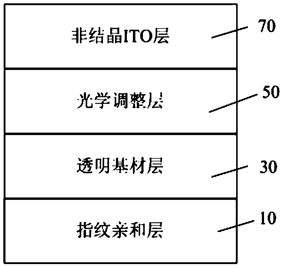
[0049] The surface of the transparent substrate layer 30 is coated with an acrylic resin layer, dried and cured to form the fingerprint affinity layer 10 .
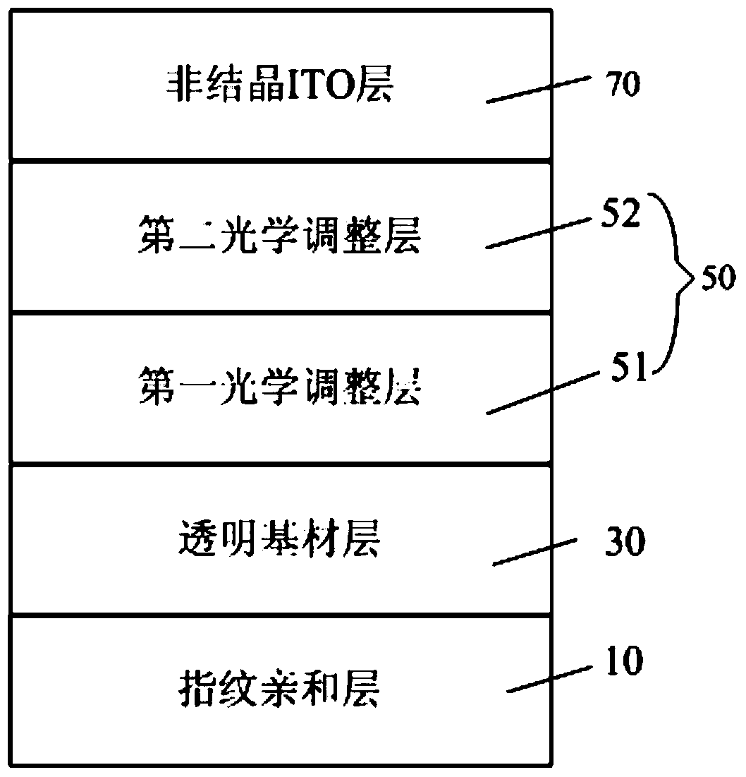
[0050] Using the sputtering method, the first optical adjustment layer 51, the second optical adjustment layer 52 and the amorphous ITO layer 70 are arranged on the surface of the transparent substrate layer 30 away from the above-mentioned fingerprint affinity layer 10 to form figure 2 The transparent conductive film shown.
[0051] The amorphous ITO layer 70 of the transparent conductive film was etched by an ink screen printing etching method, and then baked at a temperature of 150° C. for 60 minutes. The specific structural parameters of the transparent conductive film are shown in Table 1.
Embodiment 2
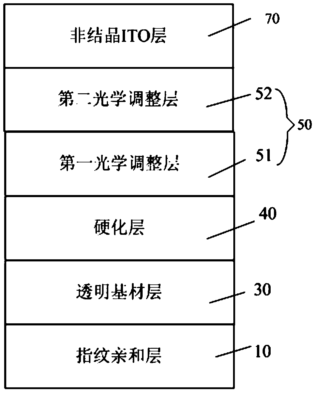
[0053] The surface of the transparent substrate layer 30 is coated with a hardening solution selected from Japan Arakawa Chemical Co., Ltd., model number FZ001, dried and cured to form a fingerprint affinity layer 10 with a film thickness of 5.0 μm. Then, in the same way, on the surface of the transparent substrate layer 30 away from the above-mentioned fingerprint affinity layer 10, the hardening solution selected from the model PC13-1082 of DIC Corporation in Japan is coated to form a hardening layer 40 with a film thickness of 0.3 μm. .
[0054] Using a magnetron sputtering process, a film is coated on the surface of the hardened layer 40 away from the above-mentioned transparent substrate layer 30, and the first optical adjustment layer 51, the second optical adjustment layer 52 and the amorphous ITO layer 70 are sequentially obtained, forming image 3 The transparent conductive film shown.
[0055] The ITO layer of the transparent conductive film was etched by an ink scr...
Embodiment 3
[0057] Adopt the method identical with embodiment 1 to prepare image 3 For the transparent conductive film shown, the structural parameters of the prepared transparent conductive film are shown in Table 1, wherein the hardening solution for coating the fingerprint affinity layer 10 is the hardening solution of FZ001 from Japan Arakawa Chemical Co., Ltd., and the coating hardening layer 40 The hardening solution used is the PC13-1082 hardening solution from DIC Corporation of Japan, and the specific structural parameters of the transparent conductive film are shown in Table 1.
PUM
 Abstract
Description
Claims
Application Information


