Array substrate and manufacturing method thereof, display panel and display apparatus

An array substrate and substrate substrate technology, which is applied in semiconductor/solid-state device manufacturing, semiconductor devices, electrical components, etc., can solve the problems of complex array substrate fabrication process, high power consumption, large parasitic capacitance, etc., and reduce parasitic capacitance. , the effect of reducing power consumption and reducing the number of masks

Active Publication Date: 2015-10-07
BOE TECH GRP CO LTD
View PDF6 Cites 20 Cited by
  • Summary
  • Abstract
  • Description
  • Claims
  • Application Information

AI Technical Summary

Problems solved by technology

[0005] The object of the present invention is to provide an array substrate and its preparation method, a display panel and a display device, so as to solve the complex preparation process of the array substrate in the prior art and the parasitic capacitance between the gate electrode and the source-drain electrode of the thin film transistor on the array substrate. Larger, causing problems with higher power consumption

Method used


Image

  • Array substrate and manufacturing method thereof, display panel and display apparatus
  • Array substrate and manufacturing method thereof, display panel and display apparatus
  • Array substrate and manufacturing method thereof, display panel and display apparatus

Examples


Embodiment Construction

[0042] The implementation process of the embodiment of the present invention will be described in detail below in conjunction with the accompanying drawings. It should be noted that the same or similar reference numerals represent the same or similar elements or elements having the same or similar functions throughout. The embodiments described below by referring to the figures are exemplary only for explaining the present invention and should not be construed as limiting the present invention.

[0043] Implementation one

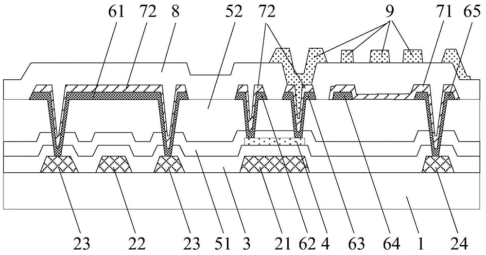
[0044] see figure 1 , an embodiment of the present invention provides an array substrate, including a base substrate 1, a gate metal layer, a gate insulating layer 3, an active layer 4, an etch stop layer 51, a source The drain metal layer, the common electrode layer, the passivation layer 8 and the pixel electrode layer, and an organic insulating layer 52 is arranged between the etching barrier layer 51 and the source-drain metal layer;

[0045] The gat...


PUM


Abstract

The invention discloses an array substrate and a manufacturing method thereof, a display panel and a display apparatus. In the prior art, a manufacturing technology of the array substrate is complex and a stray capacitance between a gate electrode and source and drain electrodes of a film transistor is large so that power consumption is large. By using the array substrate and the manufacturing method thereof, the display panel and the display apparatus of the invention, the above problems are solved. The array substrate comprises a gate metal layer, a gate insulation layer, an active layer, an etching barrier layer, a source and drain metal layer, a common electrode layer, a passivation layer and a pixel electrode layer which are successively formed on a substrate. An organic insulating layer is arranged between the etching barrier layer and the source and drain metal layer. The gate metal layer comprises the gate electrode, a gate line and a data line, wherein the gate line and the data line are arranged in a cross mode. The gate electrode is located below the active layer. The data line is separated into several segments by the gate line. The source and drain metal layer comprises a source electrode, a drain electrode and a plurality of first connecting lines. The source electrode and the drain electrode are located above the active layer and are connected to the active layer through first through holes of different positions respectively. The several segments of each data line are connected into one body through the plurality of first connecting lines.

Description

technical field [0001] The invention relates to the field of liquid crystal display, in particular to an array substrate and a preparation method thereof, a display panel and a display device. Background technique [0002] Among flat panel display devices, Thin Film Transistor Liquid Crystal Display (TFT-LCD for short) has the characteristics of small size, low power consumption, relatively low manufacturing cost and no radiation. occupied a dominant position. [0003] Array substrate is one of the important components of TFT-LCD. A liquid crystal layer is set between the array substrate and the color filter substrate. By applying voltage to the common electrodes and pixel electrodes on the array substrate, the arrangement of liquid crystal molecules can be changed to control the transmission of light. Different voltages are set on each pixel. And with a uniform backlight, it can realize the display of different gray scales. Through the combination of red, green and blue c...

Claims


Application Information

Patent Timeline
Patent Type & Authority Applications(China)
IPC IPC(8): H01L27/12H01L21/77
Inventor 舒适张斌何晓龙
Owner BOE TECH GRP CO LTD
Why Eureka
Try Eureka