Semiconductor laser multi-chip sintering clamp and sintering method

A technology of lasers and semiconductors, which is applied in semiconductor lasers, lasers, laser parts, etc., can solve the problems of high price of automation equipment, influence on the uniformity of applied force, and unsuitability for mass production, so as to reduce the probability of void generation, facilitate operation, The effect of high sintering efficiency

Active Publication Date: 2015-10-07
Shandong Huaguang Optoelectronics Co. Ltd.
View PDF5 Cites 16 Cited by
  • Summary
  • Abstract
  • Description
  • Claims
  • Application Information

AI Technical Summary

Problems solved by technology

The fixture adopts the pressure method of shrapnel to apply force. Because the shrapnel is easy to deform, it will affect the uniformity of the force after repeated use.
[0005] At present, the sintering of lasers is generally complet

Method used


Image

  • Semiconductor laser multi-chip sintering clamp and sintering method
  • Semiconductor laser multi-chip sintering clamp and sintering method
  • Semiconductor laser multi-chip sintering clamp and sintering method

Examples


Embodiment 1

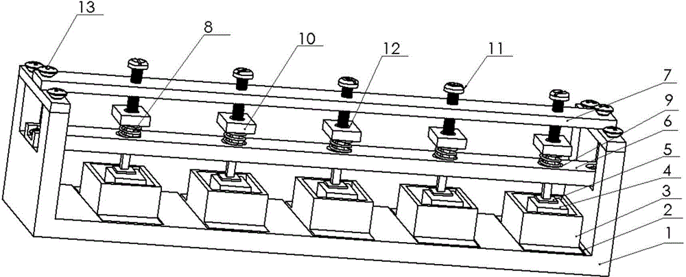
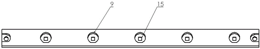
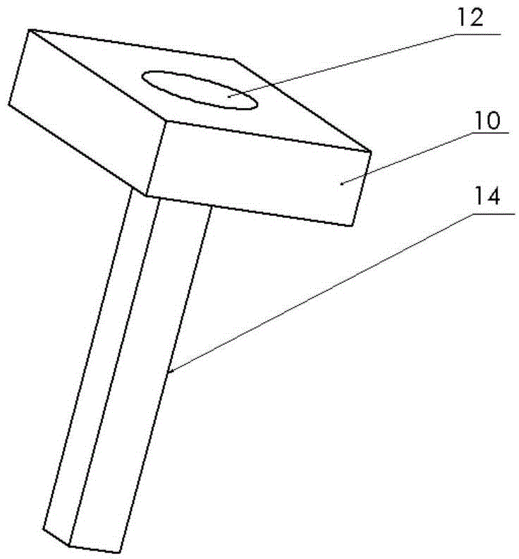
[0044] Semiconductor laser multi-chip sintering fixture, the structure is as follows figure 1As shown, it includes a main body 1, a lower pressing bar 6, an upper pressing bar 7, a top block 10 and a spring 8. The main body 1 is composed of a bottom plate and a side plate. The laser tube shell 3 is used to prevent the laser tube shell 3 from being displaced before and during sintering. The lower bead 6 and the upper bead 7 are rectangular strips, and a lower bead 6 and an upper bead 7 are fixed on the side plate of the main body 1 by fixing screws 13 at both ends, and are parallel to the surface of the main body bottom plate; the upper bead 7 There are 5 uniformly distributed thread holes on the top for screwing in the feed screw 11 and limiting the position; the lower pressure bar 6 is provided with 5 evenly distributed column holes 15, and the top block pressure column 14 passes through the column holes To extend to the bottom; the column holes of the lower bead and the thr...

Embodiment 2

[0048] A kind of method that semiconductor laser is carried out multi-chip sintering, utilizes the sintering jig described in embodiment 1, and the steps are as follows:

[0049] (1) Place the heat sink 4 whose upper surface has been prefabricated with solder into the laser tube shell 3 with solder;

[0050] (2) Place the COS 5 at the designated position of the above-mentioned heat sink 4 to ensure that the light output position meets the requirements;

[0051] (3) Place the laser tube shells with the heat sink and COS placed in the laser limiting groove 2 of the main body one by one, ensuring that the upper force point of the COS is directly below the top block pressure column 14;

[0052] (4) Rotate the feed screws 11 one by one, move the top block pressure column 14 down through spring compression, and press the bottom of the top block pressure column 14 to the point of force on the COS. When the screw is fed, ensure that its top is located at the feed screw In the limit g...

Embodiment 3

[0057] A semiconductor laser multi-chip sintering fixture, as described in Embodiment 1, the difference is that the surface of the main body 1 bottom plate is provided with two rows of laser limiting grooves 2, each row of 5 laser limiting grooves, the structure is as follows Figure 4 shown. Correspondingly, the lower pressing bar is two rectangular strips side by side, and the upper pressing bar is also two side-by-side rectangular strips. Align top and bottom. The number of chips that can be simultaneously sintered by this jig is twice that of the jig in Example 1.


PUM


Abstract

The invention relates to a semiconductor laser multi-chip sintering clamp and a sintering method. The sintering clamp comprises a main body, a lower pressing bar, an upper pressing bar, top blocks with pressing columns and springs. The lower pressing bar and the upper pressing bar are fixed on the main body through fixing screws; the lower pressing bar and the upper pressing bar are provided with holes which are evenly distributed and are used for limiting the top block pressing columns and feeding screws; a spring sleeves the top block pressing column; the bottom of the main body is provided with laser limitation grooves. The sintering method comprises steps of successively placing the tube casings containing heat sinks and COSs in the laser limitation grooves and the positions below the top block pressing columns, transmitting to feeding screws to enable the pressing columns to descend to the bottom and to contact with the COSs, clamping the chip by applying pressure, and performing sintering on the clamp, on which the laser is installed. The pressing column of the invention is of a square structure and maintains no rotation during the pressing down, preventing the displacement of the COS in the installation process and improving the consistency of sintering. At the meantime, the clamp is provided with a plurality of lasers according to the needs, which is high in sintering and easy to industrialization.

Description

technical field [0001] The invention relates to a sintering jig for a semiconductor laser, in particular to a jig capable of simultaneously pressurizing and sintering multiple chips, and belongs to the technical field of semiconductor laser sintering. Background technique [0002] Due to the advantages of small size, light weight, high conversion efficiency and long service life, semiconductor lasers are widely used in medical, display, pumping, industrial processing and other fields. In recent years, with the rapid development of semiconductor material epitaxial growth technology, semiconductor laser waveguide structure optimization technology, cavity surface passivation technology, high stability packaging technology, and efficient heat dissipation technology, especially in the direct semiconductor laser industrial processing applications and high-power optical fiber Driven by the demand for laser pumping, semiconductor lasers with high power and high beam quality have dev...

Claims


Application Information

Patent Timeline
IPC IPC(8): H01S5/024H01S5/022
Inventor 孙素娟杨扬于果蕾江建民
Owner Shandong Huaguang Optoelectronics Co. Ltd.
Why Eureka
Try Eureka