Method for heat treatment of silicon wafer and silicon wafer

A heat treatment method and technology for silicon wafers, applied in the directions of post-processing, post-processing details, chemical instruments and methods, etc., can solve problems such as inability to ensure wafer in-plane uniformity, BMD density difference, etc., and achieve the effect of improving strength and gettering effect of ability

Active Publication Date: 2015-10-14
GLOBALWAFERS JAPAN
View PDF4 Cites 4 Cited by
  • Summary
  • Abstract
  • Description
  • Claims
  • Application Information

AI Technical Summary

Problems solved by technology

Therefore, even if heat treatment is performed on a wafer cut out from this crystal, almost no BMD is formed, and there arises a problem that there is a difference in BMD density between the vicinity of the OSF ring region and other regions, and the in-plane uniformity of the wafer cannot be ensured. sex

Method used


Image

  • Method for heat treatment of silicon wafer and silicon wafer
  • Method for heat treatment of silicon wafer and silicon wafer
  • Method for heat treatment of silicon wafer and silicon wafer

Examples


Embodiment Construction

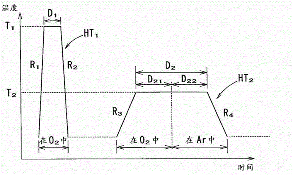
[0053] (1) heat treatment sequence of the invention of the present application

[0054] figure 1 An example of the procedure of the heat treatment method of the silicon wafer (hereinafter referred to as wafer) of the present invention is shown in . This heat treatment method is performed by continuously performing the first heat treatment HT using a lamp annealing furnace. 1 and the second heat treatment HT using a batch heat treatment furnace 2 These two heat treatments are formed.

[0055] Although not shown in this figure, in the first heat treatment HT 1 Thereafter, a step of peeling off the oxide film formed on the wafer surface is provided. This peeling step may also be omitted. In addition, in the second heat treatment HT 2 Thereafter, both front and back surfaces of the wafer are ground (about 5 to 6 μm per side) and single side grinding (about 1 μm) of the wafer surface is performed. By performing this polishing, the roughness of the wafer can be improved, and ...


PUM

PropertyMeasurementUnit
diameteraaaaaaaaaa
sizeaaaaaaaaaa

Abstract

The present invention aims to ensure the strength of a surface layer and a main body of a silicon wafer, and enhance the in-plane homogeneity of crystal quality. A method for heat treament of silicon wafer includes the steps as follows: firstly, heat treating silicon wafers in an oxidizing atmosphere in a temperature range between 1300 DEG C to 1400 DEG C; secondly, cooling the heat-treated silicon wafers at a speed of 10 DEG C per second to 150 DEG C per second; and thirdly, heat treating the cooled silicon wafers in the oxidizing atmosphere in a temperature range between 800 DEG C to 1250 DEG C for one hour to one hundred hours.

Description

technical field [0001] The present invention relates to a heat treatment method of a silicon wafer cut out from a silicon ingot grown by a pulling method and a silicon wafer thereof. Background technique [0002] In recent years, with the high integration of semiconductor devices, the crystal integrity of the device active region (from the surface to the depth region of about 7 μm) on the surface layer of the silicon wafer (hereinafter referred to as wafer) used as the substrate has been greatly reduced. Quality requirements such as improvement, ensuring sufficient mechanical strength of the wafer surface layer and the wafer interior (referring to parts other than the wafer surface layer, hereinafter referred to as the main body), and overall quality uniformity in the wafer surface have become more stringent. [0003] In order to improve crystal integrity, heat treatment in a batch heat treatment furnace maintained at a high temperature is performed, as disclosed in Patent D...

Claims


Application Information

Patent Timeline
Patent Type & Authority Applications(China)
IPC IPC(8): H01L21/324H01L21/322C30B33/02C30B29/06
Inventor 须藤治生荒木浩司青木龙彦前田进
Owner GLOBALWAFERS JAPAN
Why Eureka
Try Eureka