Shielding film, shielding circuit board and terminal device

A technology for shielding circuits and shielding films, applied in circuit devices, printed circuit parts, magnetic field/electric field shielding, etc., can solve the problems of gaps in pins, electromagnetic leakage, difficulty in adapting to ultra-thin design requirements, etc., to reduce the thickness , the effect of preventing short circuit

Active Publication Date: 2015-10-14
HUAWEI DEVICE CO LTD
View PDF4 Cites 21 Cited by
  • Summary
  • Abstract
  • Description
  • Claims
  • Application Information

AI Technical Summary

Problems solved by technology

[0003] The metal shielding cover in the prior art has the following defects: firstly, when using a crimping method to connect to the grounding pad, the metal shielding cover contacts the grounding pad with a relatively large area, so as to facilitate the connection with connectors such as screws. It will cause the size of the metal shield and the grounding pad to be too large, which is not conducive to the high-density installation of electronic components on the circuit board to achieve thinning of electronic products; when connecting to the grounding pad by welding, in order to ensure high flatness , it is necessary to set several pins spaced apart from each other at the lower end of the metal shield, and solder them to the ground pad through the pins. When using the

Method used


Image

  • Shielding film, shielding circuit board and terminal device
  • Shielding film, shielding circuit board and terminal device
  • Shielding film, shielding circuit board and terminal device

Examples


Embodiment 1

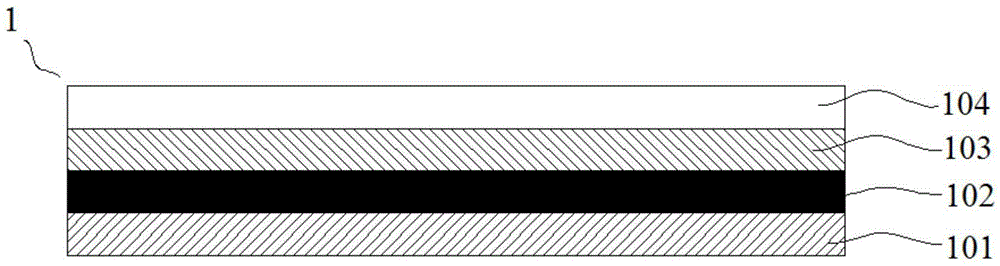
[0037] refer to figure 2 , figure 2 It is a specific embodiment of the shielding film in the embodiment of the present invention. The shielding film 1 described in this embodiment includes a first insulating layer 101 and a shielding layer 102. The shielding layer 102 is arranged on the first insulating layer 101. The first insulating layer 101 It is made of flexible insulating material or anisotropic conductive material, and the shielding layer 102 is made of conductive material or magnetically conductive material.

[0038]The shielding film 1 described in this embodiment has a multilayer structure, the first insulating layer 101 is a flexible insulating material or an anisotropic conductive material, and the shielding layer 102 is a conductive material, so that the electronic components of the circuit board are shielded by the shielding film 1 , the first insulating layer 101 can be pasted on the surface of the electronic component to be shielded, because the material of ...

Embodiment 2

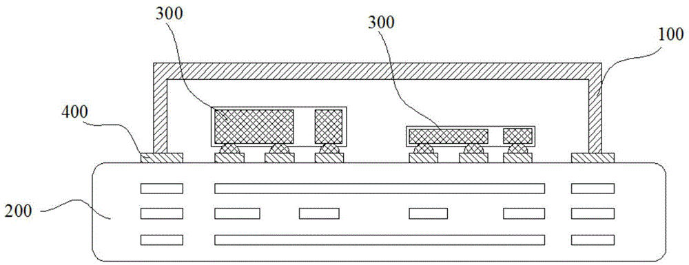
[0053] refer to Figure 5 , Figure 5 As a specific embodiment of the shielded circuit board in the embodiment of the present invention, the shielded circuit board described in this embodiment includes:

[0054] The shielding film 1, the shielding film 1 includes a first insulating layer 101 and a shielding layer 102, the shielding layer 102 is arranged on the first insulating layer 101, wherein the first insulating layer 101 is a flexible insulating material or an anisotropic conductive material, the The shielding layer 102 is a conductive or magnetically conductive material;

[0055] The circuit board 2 is provided with electronic components 3 on the circuit board 2, the shielding film 1 is covered on the electronic components 3, the first insulating layer 101 can be attached to the upper surface of the electronic components 3 of the circuit board 2, the shielding film 1 and the circuit board 2, the shielding layer 102 is connected to the grounding pad 4, and the electroni...

Embodiment 3

[0069] refer to Image 6 , Image 6 As a specific embodiment of the shielded circuit board in the embodiment of the present invention, the shielded circuit board described in this embodiment includes:

[0070] The shielding film 1, the shielding film 1 includes a first insulating layer 101 and a shielding layer 102, the shielding layer 102 is arranged on the first insulating layer 101, the first insulating layer 101 is a flexible insulating material or an anisotropic conductive material, and the shielding layer 102 is conductive or magnetically conductive material;

[0071] The circuit board 2 is provided with electronic components 3 on the circuit board 2, the shielding film 1 is covered on the electronic components 3, the first insulating layer 101 can be attached to the upper surface of the electronic components 3 of the circuit board 2, the shielding film 1 and the circuit board 2, the shielding layer 102 is connected to the grounding pad 4, and the electronic component ...


PUM

PropertyMeasurementUnit
Thicknessaaaaaaaaaa
Thicknessaaaaaaaaaa
Thicknessaaaaaaaaaa

Abstract

The present invention relates to the technical field of electromagnetic shielding. Disclosed in an embodiment of the present invention are a shielding film, shielding circuit board and terminal device, being capable of improving the electromagnetic shielding effect, decreasing product thickness and improving heat dissipation performance. The shielding film comprises a first insulating layer and a shielding layer located over the first insulating layer, the first insulating layer being of flexible insulative material or anisotropic conductive material, and the shielding layer being of electrically conductive or magnetically conductive material.

Description

technical field [0001] The invention relates to the technical field of electromagnetic shielding, in particular to a shielding film, a shielding circuit board and terminal equipment. Background technique [0002] Electromagnetic shielding technology refers to the use of shields made of magnetic or conductive materials to limit electromagnetic interference energy within a certain range to control the induction or radiation of electric fields, magnetic fields, and electromagnetic waves from one area to another. Specifically, shielding is used to isolate electronic components, circuit cables, or the interference source of the entire system to prevent the influence of external electromagnetic fields or the outward diffusion of interference electromagnetic fields. At present, the electronic components in electronic devices usually need to be installed on the circuit board to form a fixed circuit, so as to meet the needs of mass production and optimized layout. When electromagneti...

Claims


Application Information

Patent Timeline
IPC IPC(8): B32B15/08B32B15/082B32B15/088B32B15/09B32B15/04H05K9/00H05K1/02
CPCH05K9/00B32B15/08B32B15/04B32B15/082B32B15/088B32B15/09B32B2307/202B32B2307/206B32B2307/212B32B2457/08H05K1/0213H05K9/0084
Inventor 沈晓兰孙宁波王玉忠杨阳狄伟周静
Owner HUAWEI DEVICE CO LTD
Why Eureka
Try Eureka