Vertically-stacked strain Si/SiGe heterojunction CMOS device structure and preparation method thereof

A device structure and heterojunction technology, which is applied in semiconductor/solid-state device manufacturing, semiconductor devices, electrical components, etc., can solve the problems of limiting device performance, hole mobility is lower than electron mobility, etc., to improve integration, The effect of increasing chip speed and reducing the area on the SiCMOS technology layout

Active Publication Date: 2015-10-21
XIDIAN UNIV
View PDF4 Cites 12 Cited by
  • Summary
  • Abstract
  • Description
  • Claims
  • Application Information

AI Technical Summary

Problems solved by technology

With the continuous improvement of integrated circuit integration and the continuous reduction of feature size, a series of problems in materials, device physics, device structure and process technology have emerged, especially due to the hole mobility ratio of bulk Si material to electron mobility. Low, the performance of Si CMOS circuits is largely restricted by p-MOSFETs, which limits the further improvement of device performance

Method used


Image

  • Vertically-stacked strain Si/SiGe heterojunction CMOS device structure and preparation method thereof
  • Vertically-stacked strain Si/SiGe heterojunction CMOS device structure and preparation method thereof

Examples


Embodiment Construction

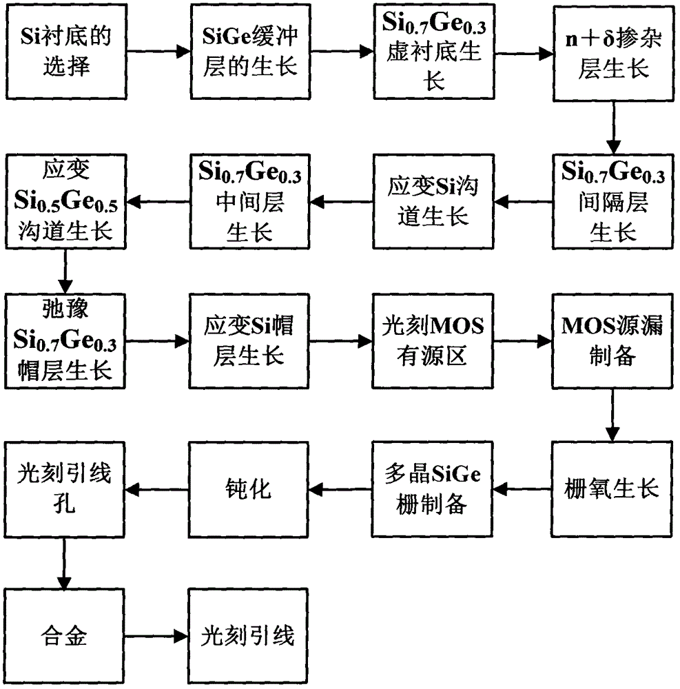
[0038] In order to make the objects and advantages of the present invention clearer, the present invention will be further described in detail below in conjunction with the examples. It should be understood that the specific embodiments described here are only used to explain the present invention, not to limit the present invention.

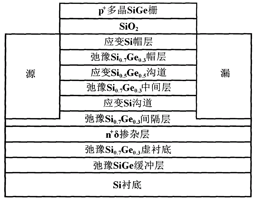
[0039] Such as figure 2 As shown, the embodiment of the present invention provides a vertically stacked strained Si / SiGe heterojunction CMOS device structure, which includes a silicon substrate, a relaxed SiGe buffer layer, and a relaxed SiGe buffer layer from bottom to top. 0.7 Ge 0.3 virtual substrate, n + δ-doped layer, relaxed Si 0.7 Ge 0.3 spacer, strained Si channel, relaxed Si 0.7 Ge 0.3 Intermediate layer, strained Si 0.5 Ge 0.5 channel, relaxed Si 0.7 Ge 0.3 capping and strained Si capping; relaxed Si 0.7 Ge 0.3 On the spacer layer, there is a source on the left, and a drain on the right. 0.7 Ge 0.3 Intermediate layer, st...


PUM


Abstract

The invention discloses a vertically-stacked strain Si/SiGe heterojunction CMOS device structure and a preparation method thereof. The device comprises a silicon substrate, a relaxation SiGe buffer layer, a relaxation Si0.7Ge0.3 virtual substrate, an n<+> delta doping layer, a relaxation Si0.7Ge0.3 interval layer, a strain Si trench, a relaxation Si0.7Ge0.3 intermediate layer, a strain Si0.5Ge0.5 trench, a relaxation Si0.7Ge0.3 cap layer and a Si cap layer from the bottom up in sequence. An n-MOSFET trench adopts a tensile strain Si material, a p-MOSFET trench adopts a compression strain SiGe material, and the n-MOSFET and the p-MOSFET adopt a vertically-stacked structure, and share one polycrystalline SiGe gate electrode, so that electron and hole migration rates are improved greatly, speed and integration level of chips are improved, and new technological approaches are provided for high speed and high frequency development of the Si device and an integrated circuit.

Description

technical field [0001] The invention relates to the technical field of semiconductor device preparation, in particular to a vertically stacked strained Si / SiGe heterojunction CMOS device structure and a preparation method thereof. Background technique [0002] Semiconductor integrated circuits are the foundation of the electronics industry, and people's huge demand for the electronics industry has prompted the rapid development of this field. In the past few decades, the rapid development of the electronics industry has had a huge impact on social development and national economy. At present, the electronics industry has become the largest industry in the world, occupying a large share in the global market, and its output value has exceeded 1 trillion US dollars. [0003] Si CMOS integrated circuits have the advantages of low power consumption, high integration, low noise and high reliability, and occupy a dominant position in the semiconductor integrated circuit industry. ...

Claims


Application Information

Patent Timeline
Patent Type & Authority Applications(China)
IPC IPC(8): H01L27/092H01L21/8238H01L29/165H01L29/78
Inventor 舒斌吴继宝范林西陈景明张鹤鸣宣荣喜胡辉勇宋建军王斌
Owner XIDIAN UNIV
Why Eureka
Try Eureka