
Method of enhancing dopant incorporation in epitaxial film using halogen molecules as reactant in depostion

A technology of dopants and halogen atoms, which is applied in the fields of electrical components, semiconductor/solid-state device manufacturing, circuits, etc., and can solve problems such as time-consuming, complicated, and affecting throughput and productivity

Inactive Publication Date: 2015-11-11
APPLIED MATERIALS INC
View PDF6 Cites 0 Cited by
  • Summary
  • Abstract
  • Description
  • Claims
  • Application Information

AI Technical Summary

Problems solved by technology

While the film growth rate or deposition efficiency of the deposition process gas can be controlled or manipulated by alternately utilizing the etch reaction to perform the deposition reaction, or by separately introducing the etch chemical and the deposition process gas into the reaction chamber under controlled time and process conditions , but this method is complex and time-consuming, thereby affecting throughput and overall productivity

Method used


Image

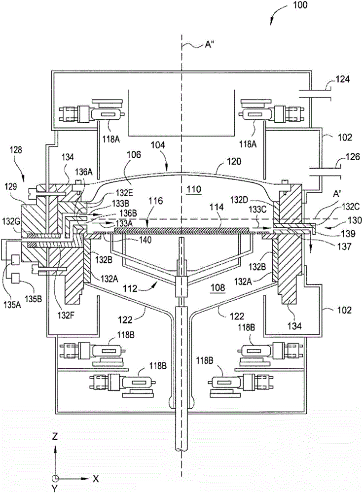
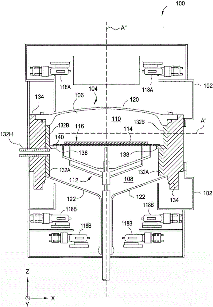
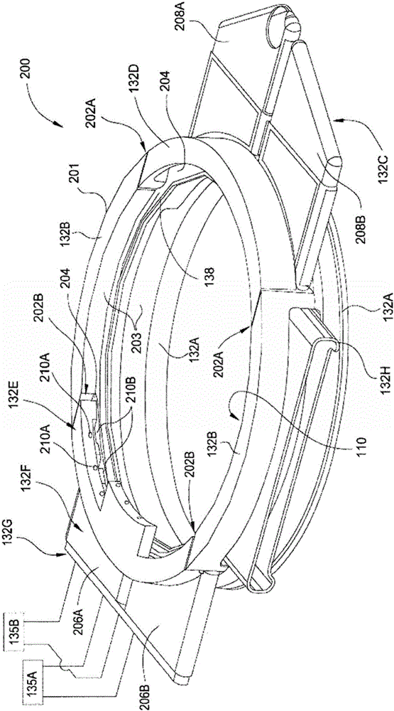
  • Method of enhancing dopant incorporation in epitaxial film using halogen molecules as reactant in depostion
  • Method of enhancing dopant incorporation in epitaxial film using halogen molecules as reactant in depostion
  • Method of enhancing dopant incorporation in epitaxial film using halogen molecules as reactant in depostion

Examples


example 7

[0057] Example 7 shows another example in which the flow rates of phosphine and chlorine are increased compared to Example 1, and the pH 3 From 5.1sccm to 15sccm and chlorine gas from 0sccm to 150sccm. It can be seen that the resulting phosphorus-doped silicon epitaxial layer has a tensile strain significantly increased from 0.03% to 0.70%. At the same time, the resulting layer had a resistivity of about 0.3 mΩ-cm, compared to 0.838 mΩ-cm for the layer in Example 1. layer thickness from increased to This again confirms that chlorine does not affect the overall film growth rate, but rather enhances the epitaxial layer with higher tensile strain and lower resistivity.

[0058] It should be noted that the examples given in Table 1 are based on a chamber pressure of 40 Torr, although higher flow rates of the phosphorus source gas may improve the tensile strain and resistivity of the deposited epitaxial layer. The high flow of phosphorus source gas provided during low pressur...


PUM


Abstract

The embodiment of the invention generally relates to a method for forming a silicon epitaxial layer on a semiconductor device. The method provided by the invention comprises heating a substrate disposed in a processing volume of a processing cavity, and exposing the substrate in a catalyst gas or one or more than one deposition gases to perform a deposition technology so as to form the silicon epitaxial layer on the substrate. The catalyst gas comprises halogen molecules, and the one or more than one deposition gases comprise a silicon source and the sources of a dopant. In one embodiment, the catalyst gas comprises chlorine.

Description

technical field [0001] Embodiments of the present invention relate generally to the field of semiconductor fabrication processes and devices, and more particularly, to methods of depositing silicon-containing films for use in forming semiconductor devices. Background technique [0002] The reduction in size of metal-oxide-semiconductor field-effect transistors (MOSFETs) enables continuous improvements in speed performance, density, and cost per function of integrated circuits. The semiconductor industry is also in a period of transition from generally planar 2D transistors to 3D transistors using three-dimensional gate structures. In a 3D gate structure, the channel, source and drain rise from the substrate, and then the gate surrounds the channel on three sides. The goal is to confine current flow to only the raised channel, as well as eliminate any possible paths for leaking electrons. One such type of 3D transistor is called a Fin Field-Effect Transistor (FinFET), in wh...

Claims


Application Information

Patent Timeline
IPC IPC(8): H01L21/02
Inventor 李学斌阿布舍克·杜贝金以宽
Owner APPLIED MATERIALS INC
Learn More