Minimized high-isolation ceramic packaging structure

A high isolation, ceramic packaging technology, used in semiconductor/solid-state device components, semiconductor devices, electrical components, etc., can solve problems such as high crosstalk and coupling effects in transmission channels, limited wiring space, increased signal loss, etc., to reduce Crosstalk and coupling effect, effect of reducing influence, reducing signal loss

Active Publication Date: 2015-11-11
CHENGDU CORPRO TECH CO LTD
View PDF9 Cites 4 Cited by
  • Summary
  • Abstract
  • Description
  • Claims
  • Application Information

AI Technical Summary

Problems solved by technology

Due to the limited wiring space of the bonding fingers, the RF bonding fingers are often not isolated from the left and right, and there are high crosstalk and coupling effects between the transmission channels, which will increase the loss of the signal and result in low isolation.

Method used


Image

  • Minimized high-isolation ceramic packaging structure
  • Minimized high-isolation ceramic packaging structure
  • Minimized high-isolation ceramic packaging structure

Examples


Embodiment 1

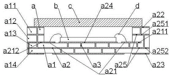
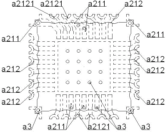
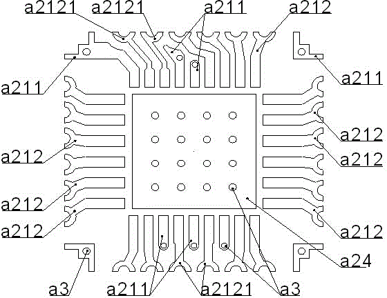
[0024] Example one : Such as figure 1 As shown, a miniaturized high isolation ceramic package structure includes a shell a, a chip b, a metal cover c, and a bonding wire d; the shell a is composed of a ceramic layer a1, a metallization layer a2, and an interconnection blind hole a3 The metallization layer a2 is composed of the bonding finger layer a21, the sealing area a22, the connection area a23, the sticky core area a24 and the printed line layer a25; the center of the shell a is provided with a sticky core for placing the chip b Area a24; the core area a24 is surrounded by a bonding finger layer a21; the bonding finger layer a21 includes a ground bonding finger a211 and a signal bonding finger a212, and the ground bonding finger a211 is connected to a blind hole a3 through an interconnection The printed line layer a25, the sealing area a22 and the sticky core area a24 are connected, and the signal bonding finger a212 is connected to the connection area a23.

[0025] The metal...

Embodiment 2

[0031] Embodiment two: such as Figure 4 As shown, the difference from the first embodiment is that the core-sticking area a24 and the second printed line layer a252 are in the same layer. Compared with the first embodiment, the advantage is that the thickness of the shell a can be reduced, but at the same time the mechanical reliability of the shell a can be reduced. Therefore, this form is mainly used for the occasions where the outer shape of the shell a is small and the thickness of the shell a is relatively high.

Embodiment 3

[0032] Example three: such as Figure 5 As shown, the difference from the first embodiment is that the signal bonding finger a212 is interconnected with the connection area a23 through the interconnection blind hole a3 to achieve electrical connection. Compared with the first embodiment, since there is no semicircular hole on the edge of the tube shell a, the outer shape of the tube shell a can be further reduced under the premise of ensuring the reliability of the tube shell a, and the miniaturization of the package can be realized. However, it is necessary to minimize the influence of the interconnection blind hole a3 on the mechanical properties of the package a, and the punch position needs to be moved inward, which will shorten the wiring length of the bonding finger layer a21 and increase the wiring difficulty. Therefore, this form is mainly used for occasions where isolation is not high and the external size of the shell a is relatively high.


PUM

PropertyMeasurementUnit
widthaaaaaaaaaa

Abstract

The invention discloses a minimized high-isolation ceramic packaging structure including a pipe case (a), a chip (b), a metal cover plate (c) and a bonding wire (d); the pipe case (a) is composed of a ceramic layer (a1), a metallization layer (a2) and an interconnection blind hole (a3); the metallization layer (a2) is composed of a bonding finger layer (a21), a sealing area (a22), a connection area (a23), a bonding chip area (a24) and a printed circuit board trace layer (a25); the pipe case(a) is provided in the center thereof with the bonding chip area (a24) for displacing the chip, and the circumference of the bonding chip area (a24) is provided with the bonding finger layer (a21) which includes a grounding bonding finger (a211) and a signal bonding finger (a212). The structure herein has the beneficial effects that stratum isolation technology is adopted, and space stereo-wrapping is conducted on the high-isolation bonding finger, and a space "sandwich" structure is formed; the structure can markedly reduce cross talk and coupling effect of the signal channels, reduce signal loss, increase isolation level, and reduce impact of packaging on the electrical property of the products, provided that the high reliability of the packaging is guaranteed by the structure.

Description

technical field [0001] The invention relates to the technical field of integrated circuit ceramic packaging, in particular to a miniaturized high-isolation ceramic packaging structure. Background technique [0002] As the frequency of integrated circuits becomes higher and higher, the impact of packaging on the electrical performance of products is increasing; the parasitic parameters of packaging not only affect the electrical performance of RF IOs, but also affect the work of adjacent IOs; with the post-Moore era With the continuous development, the shape of integrated circuits is getting smaller and smaller, which increases the difficulty of designing high-frequency integrated circuit ceramic shells. [0003] From the top to the bottom of the traditional ceramic shell, it is the sealing area, the ceramic layer, the bonding finger layer, the ceramic layer, and the connection area. This layout does not isolate the RF IO, which will seriously affect the electrical performan...

Claims


Application Information

Patent Timeline
Patent Type & Authority Applications(China)
IPC IPC(8): H01L23/488
CPCH01L2224/32225H01L2224/48091H01L2224/48227H01L2224/73265H01L2924/16195
Inventor 周平
Owner CHENGDU CORPRO TECH CO LTD
Why Eureka
Try Eureka