Junction termination structure of transverse high-voltage power device

A power device and lateral high voltage technology, applied in the direction of semiconductor devices, electrical components, circuits, etc., can solve the problems of power device breakdown, device withstand voltage is not the optimal value, etc., to optimize the breakdown voltage, avoid premature breakdown, Improving the effect of charge imbalance

Active Publication Date: 2015-11-11
UNIV OF ELECTRONICS SCI & TECH OF CHINA
View PDF3 Cites 8 Cited by
  • Summary
  • Abstract
  • Description
  • Claims
  • Application Information

AI Technical Summary

Problems solved by technology

However, under the triple RESURF structure device, the patent does not optimize the terminal structure of the connecting part of the straight junction terminal structure and the curvature junction terminal structure. In the connected part, due to the imbalance of charges, the power device will break down early, so the device Pressure resistance is not optimal

Method used


Image

  • Junction termination structure of transverse high-voltage power device
  • Junction termination structure of transverse high-voltage power device
  • Junction termination structure of transverse high-voltage power device

Examples


Embodiment 1

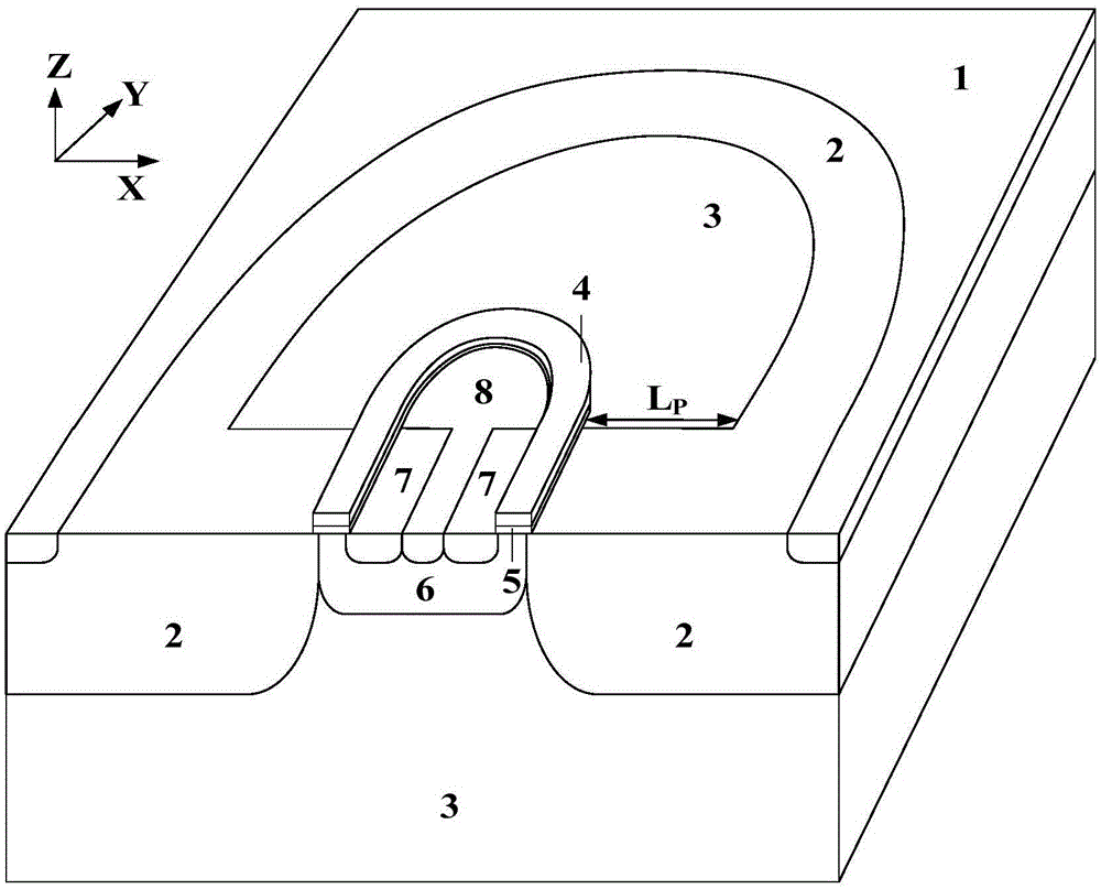
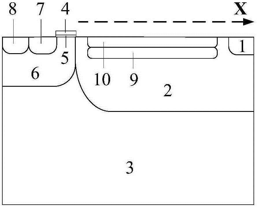
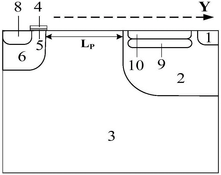
[0029] Such as Figure 5 As shown, the structure of this example includes a linear knot terminal structure and a curvature knot terminal structure;

[0030] The linear junction terminal structure is the same as that of the active region of the lateral high-voltage power device, including the drain N + Contact region 1, N-type drift region 2, P-type substrate 3, gate polysilicon 4, gate oxide layer 5, P-well region 6, source N + Contact area 7, source P + Contact region 8, P-type buried layer 9, N-type doped layer 10; P-well region 6 and N-type drift region 2 are located on the upper layer of P-type substrate 3, wherein P-well region 6 is located in the middle, and both sides are N-type The drift region 2, and the P-well region 6 is connected to the N-type drift region 2; the two sides of the N-type drift region 2 away from the P-well region 6 are the drain N + The surface of the contact region 1, the P-well region 6 has a source N connected to the metallized source + conta...

Embodiment 2

[0035] Such as Figure 6 As shown, the difference between this example and Example 1 is that the inner wall of the ring-shaped P-type buried layer 9 in the curvature junction termination structure in this example is located in the N-type drift region 2, and the principle is the same as that of Example 1.

Embodiment 3

[0037] Such as Figure 7 As shown, the difference between this example and Example 1 is that in this example, the connection between the P-type buried layer 9 and the P-type buried layer 9 in the curvature junction terminal structure is located in the N-type drift region, and the principle is the same as that of Example 1. .


PUM


Abstract

The invention belongs to the technical field of semiconductors, and particularly relates to a junction termination structure of a transverse high-voltage power device. According to the structure provided by the invention, in the connected part of a linear junction termination structure and a curvature junction termination structure, in the Y direction, a P-type buried layer exceeds an N-type drift region 5 microns; and meanwhile, the P-type buried layer also exceeds an N-type doped layer 3 microns. In an actual technology, an N-type drift region 2 is formed by ion injection; after annealing junction pushing, the N-type drift region diffuses towards the Y direction; and the P-type buried layer exceeds the N-type drift region 2 a certain distance, so that P-type impurities in the diffused N-type drift region are exhausted, therefore, the problem of unbalanced charge in the connected part of the linear junction termination structure and the curvature junction termination structure is solved, so as to obtain relatively optimized breakdown voltage. The junction termination structure has the beneficial effects that the problem of unbalanced charge in the connected part of the linear junction termination structure and the curvature junction termination structure is solved; and pre-breakdown of the device is avoided, so as to obtain the optimal breakdown voltage.

Description

technical field [0001] The invention belongs to the technical field of semiconductors, and in particular relates to a junction terminal structure of a lateral high-voltage power device. Background technique [0002] The development of high-voltage power integrated circuits is inseparable from the integration of lateral high-voltage power semiconductor devices. Lateral high-voltage power semiconductor devices are usually closed structures, including circular, racetrack and interdigitated structures. For the closed racetrack structure and the interdigitated structure, there will be small curvature terminations in the curved part and the fingertip part, and the electric field lines are easy to concentrate at the small curvature radius, which will lead to early avalanche breakdown of the device at the small curvature radius , which poses new challenges to the layout structure of lateral high-voltage power devices. [0003] The Chinese patent with publication number CN102244092...

Claims


Application Information

Patent Timeline
Patent Type & Authority Applications(China)
IPC IPC(8): H01L29/06H01L29/78
CPCH01L29/0684H01L29/78
Inventor 乔明王裕如代刚张晓菲周锌何逸涛张波
Owner UNIV OF ELECTRONICS SCI & TECH OF CHINA
Why Eureka
Try Eureka