Non-polar patterned AlN/sapphire composite substrate and manufacturing method thereof

A technology for patterning sapphire and composite substrates, which is used in semiconductor/solid-state device manufacturing, electrical components, circuits, etc., can solve large lattice mismatch and thermal mismatch, and is difficult to grow low dislocation density Group III nitrides Semiconductor materials and other issues, to achieve the effect of suppressing anisotropy, reducing stacking faults, edge and screw dislocation densities, and improving crystal quality

Active Publication Date: 2019-03-29
SOUTHEAST UNIV
View PDF9 Cites 9 Cited by
  • Summary
  • Abstract
  • Description
  • Claims
  • Application Information

AI Technical Summary

Problems solved by technology

However, due to the large lattice mismatch and thermal mismatch between the III-nitride material and the sapphire substrate, it is difficult to grow a high-quality III-nitride semiconductor material with a low dislocation density.

Method used


Image

  • Non-polar patterned AlN/sapphire composite substrate and manufacturing method thereof
  • Non-polar patterned AlN/sapphire composite substrate and manufacturing method thereof

Examples


Embodiment 1

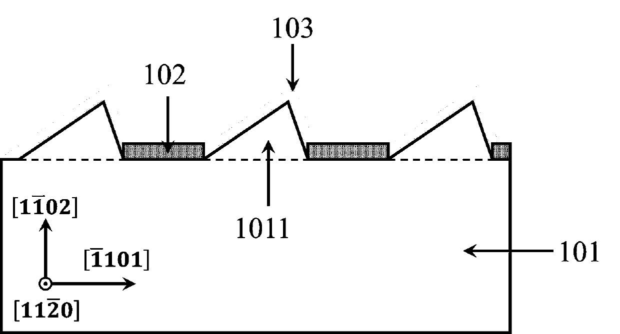
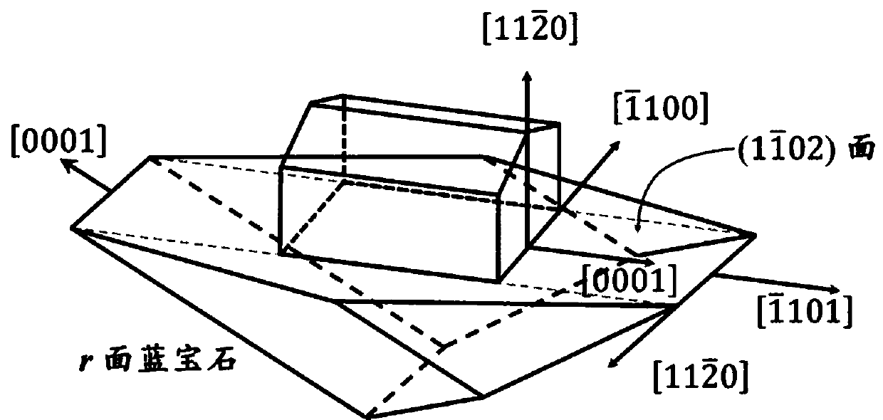
[0030] Such as figure 1 As shown, it is a schematic structural diagram of a non-polar patterned AlN / sapphire composite substrate provided by the present invention, and its structure includes an r-plane patterned sapphire substrate (101), a sapphire pattern (1011), and a mask layer (102) and AlN capping layer (103). Wherein the r-plane sapphire pattern (1011) is actually a part of the patterned r-plane sapphire substrate (101).

[0031] First, an r-plane sapphire substrate capable of epitaxially growing non-polar III-nitride materials is selected, and then an r-plane patterned sapphire substrate (101) is obtained by etching a sapphire pattern (1011) on the surface of the r-plane sapphire substrate. Among them, the sapphire pattern (1011) is an asymmetric conical structure, that is, the central axis of the conical structure is oriented The direction is inclined. The central axis of the cone is the line connecting the apex of the cone and the center of the bottom surface. The...

Embodiment 2

[0037] A non-polar patterned AlN / sapphire composite substrate is manufactured by the same process as in Example 1, except that the sapphire pattern (1011) is an asymmetric pyramid structure, that is, the pyramid structure is biased towards direction, the central axis of the pyramid is the connection line between the apex of the pyramid and the center of gravity of the bottom surface, and the angle between the central axis and the bottom surface is 60°; the mask layer (102) is deposited by the SiN on the semiconductor deposition technology x film. Other steps are the same.


PUM

PropertyMeasurementUnit
thicknessaaaaaaaaaa
thicknessaaaaaaaaaa

Abstract

The invention discloses a non-polar patterned AlN/sapphire composite substrate and a manufacturing method thereof. The structure thereof comprises a r-plane patterned sapphire substrate, a sapphire pattern, a mask layer and an AlN covering layer. The sapphire pattern is a part of the r-plane patterned sapphire substrate, and is an asymmetric conical or pyramidal structure, that is, inclines towarda [1101] crystal orientation. The structure can effectively solve a problem that crystal quality is difficult to improve since growth rates along different directions are different during epitaxial growth of non-polar III-nitride. The AlN covering layer is formed by direct reaction with NH3 while the sapphire substrate is decomposed under high temperature in an NH3 atmosphere. The composite substrate provided by the invention can effectively reduce combination of O-containing impurities in an epitaxial growth process of the III-nitride, and can also obtain a dense high-quality non-polarity AlN covering layer on the surface of the sapphire substrate on the premise of not consuming an Al source, and has important significance on growing the high-quality non-polar III-nitrides and related devices on the substrate.

Description

[0001] Field [0002] The invention belongs to the field of nonpolar nitride semiconductor materials, and in particular relates to a nonpolar patterned AlN / sapphire composite substrate and a preparation method thereof. Background technique [0003] Group III nitride materials are the third-generation semiconductor materials that emerged after the first-generation semiconductors Si, Ge and the second-generation semiconductors GaAs and InP, including GaN, InN, AlN and their ternary alloys InGaN, AlGaN, AlInN and quaternary Alloy AlInGaN. Because the band gap of III-nitride materials can be continuously adjusted between 0.7-6.2eV, it can cover the spectral range from infrared to ultraviolet, and has high breakdown voltage, high electron mobility, high thermal conductivity, high temperature resistance, It has the advantages of acid and alkali resistance and radiation resistance, so it is widely used in high voltage, high frequency, high temperature and high power optoelectronic d...

Claims


Application Information

Patent Timeline
Patent Type & Authority Applications(China)
IPC IPC(8): H01L33/32H01L33/00H01L21/86
CPCH01L21/86H01L33/007H01L33/0075H01L33/32
Inventor 张雄陈帅赵见国崔一平
Owner SOUTHEAST UNIV
Why Eureka
Try Eureka