Reinforcing sheet and process for producing semiconductor device through secondary mounting

A manufacturing method, semiconductor technology, applied in semiconductor/solid-state device manufacturing, semiconductor devices, chemical instruments and methods, etc., can solve problems such as increased injection volume, wider interval, difficulty in adjusting sealing resin injection position and injection volume, etc.

Inactive Publication Date: 2015-11-11
NITTO DENKO CORP
View PDF4 Cites 8 Cited by
  • Summary
  • Abstract
  • Description
  • Claims
  • Application Information

AI Technical Summary

Problems solved by technology

As such a sealing resin, liquid sealing resin is widely used, but since it is liquid, it is difficult to adjust the injection position and injection amount of the sealing resin, or the solder ball and the substrate may be disconnected due to the large solder ball for secondary mounting. The gap between them becomes wider and the injection volume increases

Method used


Image

  • Reinforcing sheet and process for producing semiconductor device through secondary mounting
  • Reinforcing sheet and process for producing semiconductor device through secondary mounting
  • Reinforcing sheet and process for producing semiconductor device through secondary mounting

Examples


no. 1 Embodiment approach

[0042] In the first embodiment, a description will be given of a method in which a package in which a semiconductor chip is flip-chip mounted on an interposer is used as a primary mounted semiconductor device, and backside grinding is performed as a process for the primary mounted semiconductor device.

[0043] [Process (A)]

[0044] In the step (A), a predetermined reinforcing sheet is bonded to the first main surface of the primary semiconductor device. Hereinafter, first, the reinforcing sheet will be described, and then, the manufacturing process of the secondary mounting semiconductor device using the reinforcing sheet will be described.

[0045] (enhancement sheet)

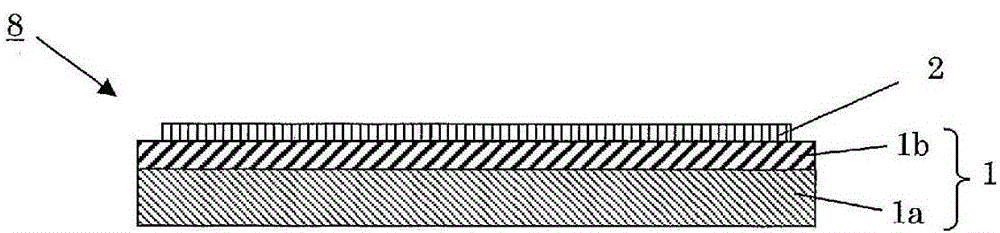
[0046] Such as figure 1 As shown, the reinforcing sheet 8 includes a base material layer 1a, an adhesive layer 1b, and a thermosetting resin layer 2 in this order. In this embodiment, the base material layer 1a and the adhesive layer 1b comprise the tape 1 for back surface grinding. Additionally, if fig...

no. 2 Embodiment approach

[0138] The primary mounting semiconductor device used in this embodiment has a target thickness, so the grinding step is omitted. Therefore, as the reinforcing sheet in the second embodiment, a reinforcing sheet including a dicing tape and a thermosetting resin layer laminated on the dicing tape is used.

[0139] [Process (A)]

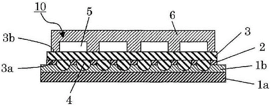
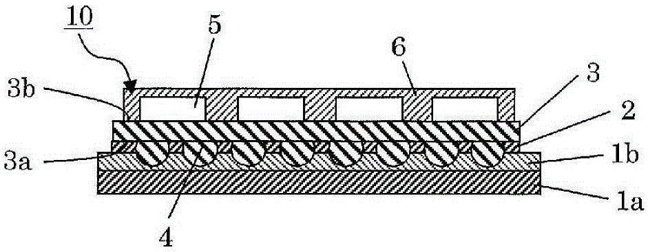
[0140] In the step (A), a predetermined reinforcing sheet is bonded to the first main surface 3 a of the primary semiconductor device 10 . The reinforcing sheet has a dicing tape 21 and a thermosetting resin layer 2 laminated on the dicing tape 21 (see Figure 3A ). The dicing tape 21 includes a base material layer 21a and an adhesive layer 21b laminated on the base material layer 21a. In addition, the thermosetting resin layer 2 is laminated on the adhesive layer 21b. As the base layer 21a, the adhesive layer 21b, and the thermosetting resin layer 2 of such a dicing tape 21, the same layers as the base layer 1a, the adhesive layer 1b, and the ther...

no. 3 Embodiment approach

[0145] In the first embodiment, as the configuration of the reinforcing sheet, the mode including the base material layer, the adhesive layer, and the thermosetting resin layer was described. In the third embodiment, the configuration of the base material layer and the adhesive layer A reinforcing sheet further provided with an intermediate layer made of a thermoplastic resin will be described. A predetermined semiconductor device can be manufactured through the same steps as in the first embodiment except that the reinforcing sheet is provided with an intermediate layer.

[0146] Such as Figure 4 As shown, the reinforcing sheet 38 includes a base material layer 31a, an intermediate layer 31c, an adhesive layer 31b, and a thermosetting resin layer 2 in this order. When the size of the protruding electrodes increases, it is necessary to increase the thickness of the thermosetting resin layer and the adhesive layer in order to realize the penetration of the protruding electrod...


PUM


Abstract

Provided is a reinforcing sheet with which it is possible to produce, through secondary mounting, a semiconductor device that has excellent impact resistance and to make steps for the secondary mounting efficient. Also provided is a process for producing a semiconductor device through secondary mounting using the reinforcing sheet. This reinforcing sheet is for reinforcing a semiconductor device produced through secondary mounting in which a semiconductor device that was produced through primary mounting and has bump electrodes formed on a first main surface thereof has been electrically connected to a wiring board through the bump electrodes. The reinforcing sheet comprises a base layer, a pressure-sensitive adhesive layer, and a thermosetting resin layer in this order, wherein the pressure-sensitive adhesive layer has a breaking strength of 0.07 MPa or greater and a melt viscosity at 60-100ºC of 4,000 Pa·s or less.

Description

technical field [0001] The present invention relates to a reinforcing sheet and a method of manufacturing a secondary mounted semiconductor device. Background technique [0002] Along with the reduction in size and thickness of electronic equipment, the demand for high-density mounting is rapidly increasing, especially in the use of portable electronic equipment such as mobile phones. Therefore, the surface mount type suitable for high-density mounting in semiconductor packages has become the mainstream instead of the conventional pin-insertion type. In this surface mount type, a semiconductor device in which a semiconductor element is resin-sealed is directly soldered to a printed circuit board for secondary mounting or the like via connection terminals such as solder balls. [0003] Here, drop impacts are often applied in portable electronic device applications, and thus impact resistance is required. In contrast, in the above-mentioned secondary mounting, in order to en...

Claims


Application Information

Patent Timeline
Patent Type & Authority Applications(China)
IPC IPC(8): H01L23/12H01L21/301H01L21/56H01L21/60
CPCH01L21/561H01L21/568H01L21/6836H01L23/3128H01L24/13H01L24/16H01L24/45H01L24/48H01L24/97H01L2221/68327H01L2221/68336H01L2221/68377H01L2221/68381H01L2224/13101H01L2224/16225H01L2224/45144H01L2224/45147H01L2224/48227H01L2924/15787H01L2221/6834B32B5/02B32B5/26B32B15/08B32B25/06B32B25/08B32B25/10B32B25/12B32B25/14B32B27/10B32B27/12B32B27/20B32B27/22B32B27/281B32B27/283B32B27/285B32B27/288B32B27/304B32B27/308B32B27/32B32B27/34B32B27/36B32B27/365B32B27/38B32B27/40B32B27/42B32B29/005B32B2255/02B32B2255/10B32B2255/12B32B2255/20B32B2255/205B32B2262/0269B32B2262/101B32B2307/50B32B2307/514B32B2307/558B32B2457/00H01L2924/181B32B7/12B32B27/08B32B2457/14H01L2221/68386H01L2924/00014H01L2924/014H01L2924/00H01L2924/00012H01L24/81H01L2221/68318H01L2224/81191
Inventor 高本尚英盛田浩介千岁裕之
Owner NITTO DENKO CORP
Why Eureka
Try Eureka