SRAM (Static Random Access Memory) time sequence control circuit with copy unit word line voltage rise technology

A timing control circuit and duplication unit technology, which is applied in the direction of digital memory information, information storage, static memory, etc., can solve the problems of inability to better improve the process deviation, increase the area of ​​the multiplying circuit, and reduce the working speed of the chip, etc., to achieve optimal The ability to resist process changes, reduce delay deviation, and increase the effect of area

Active Publication Date: 2015-11-18
ANHUI UNIVERSITY
View PDF4 Cites 3 Cited by
  • Summary
  • Abstract
  • Description
  • Claims
  • Application Information

AI Technical Summary

Problems solved by technology

[0004] In order to obtain optimal timing control, a timing replication bit line technology was proposed in 1998. Compared with the inverter chain delay technology, this technology has better resistance to process deviation and can more accurately track the bit line discharge. With the advancement of process technology, this traditional copy bit line technology can no longer improve the process deviation with the reduction of power supply voltage.
[0005] Y.Niki et al. proposed a digital replication bit line delay technology in 2011. This technology greatly improves the timing deviation at low voltage by increasing the replication unit and combining the delay multiplication circuit, but The multiplication circuit will bring a large increase in area and delay quantization error
In 2014, Y. Li et al. proposed the double-copy bit line technology, which improved the 6-tube unit and made full use of the bit line resources, which improved the circuit’s ability to resist process deviation without increasing the area. However, due to The capacitance of the bit line becomes larger, which increases the precharging time of the bit line and reduces the working speed of the chip.

Method used


Image

  • SRAM (Static Random Access Memory) time sequence control circuit with copy unit word line voltage rise technology
  • SRAM (Static Random Access Memory) time sequence control circuit with copy unit word line voltage rise technology
  • SRAM (Static Random Access Memory) time sequence control circuit with copy unit word line voltage rise technology

Examples


Embodiment

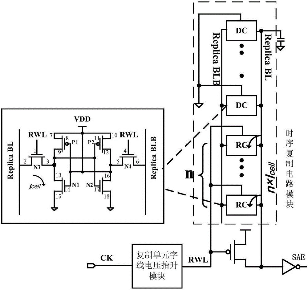
[0034] figure 1 A timing control circuit for an SRAM with the word line voltage boosting technique for replicating cells provided for an embodiment of the present invention, such as figure 1 As shown, it mainly includes: timing replication circuit module and replication cell word line voltage boosting module; where:

[0035] The timing replication circuit module is connected in parallel between the replication unit word line and the replication bit line, and is used to replicate the discharge time of the storage array, which includes n serially connected replica cells (RC) and several serially connected redundant cells (DC) ; There are two copy bit lines, such as figure 1 The replica bit lines ReplicaBL and ReplicaBLB in the replica; wherein, the two ends of all replica units are respectively connected to the replica bit lines ReplicaBL and ReplicaBLB, and the control ends of all replica units are connected to the replica unit word line (RWL); the redundancy Both ends of the...


PUM


Abstract

The invention discloses an SRAM (Static Random Access Memory) copy bit line circuit, comprising a time sequence copy circuit module and a copy unit word line voltage rise module, wherein the time sequence copy circuit module is connected in parallel between a copy unit word line and a copy bit line; one end of the copy unit word line voltage rise module is connected with a clock signal end, the other end of the copy unit word line voltage rise module is connected with the copy unit word line, and the copy unit word line voltage rise module is used for processing an input clock signal into a high-voltage level signal and transmitting the level signal to the copy unit word line; and the higher the voltage of the copy unit word line is, the larger the current and deviation of a discharge unit are, the smaller the delay deviation of a time sequence control circuit is. The circuit provided by the invention has very good process deviation resistance under low power voltage, cannot greatly increase the area of a chip, and does not influence the operational speed of the chip.

Description

technical field [0001] The invention relates to the technical field of integrated circuit (IC) design, in particular to an SRAM timing control circuit with word line voltage raising technology for replicating cells. Background technique [0002] In modern society, due to the rapid development of mobile communication technology, 3D technology, GPS navigation technology and high-speed wireless network technology, IC design is driven to pursue faster speed, higher stability and lower power consumption. SRAM (Static Random Access Memory) occupies the main area of ​​on-chip memory because of its high speed, low power consumption and high robustness, so the performance of SRAM seriously affects the function of SoC chip. [0003] At this stage, the power consumption is mainly reduced by reducing the operating voltage of the SRAM, because for the SRAM, the power consumption is linearly related to the square of the low voltage of the power supply. However, as the power supply voltag...

Claims


Application Information

Patent Timeline
Patent Type & Authority Applications(China)
IPC IPC(8): G11C11/413
Inventor 李正平尚凤仪谢明明李颂卢文娟周永亮彭春雨谭守标陈军宁
Owner ANHUI UNIVERSITY
Why Eureka
Try Eureka