Chip DRAM (dynamic random access memory) pad arrangement structure for improving encapsulation compatibility

A compatibility, pad technology, applied in electrical components, electrical solid devices, circuits, etc., can solve problems such as low compatibility, achieve strong compatibility, and improve package compatibility.

Active Publication Date: 2015-11-18
ALLWINNER TECH CO LTD
View PDF5 Cites 2 Cited by
  • Summary
  • Abstract
  • Description
  • Claims
  • Application Information

AI Technical Summary

Problems solved by technology

The existing chip pad layout design generally only considers supporting a single chip package
The key point of chip package compatible design is chip pad design. The existing pad design only supports single chip package, which makes the compatibility between SIP design and single chip package design low.

Method used


Image

  • Chip DRAM (dynamic random access memory) pad arrangement structure for improving encapsulation compatibility
  • Chip DRAM (dynamic random access memory) pad arrangement structure for improving encapsulation compatibility
  • Chip DRAM (dynamic random access memory) pad arrangement structure for improving encapsulation compatibility

Examples


Embodiment Construction

[0020] In order to make the purpose, technical solution and advantages of the present invention clearer, the chip DRAM pad layout structure and specific implementation methods for improving packaging compatibility of the present invention will be described below with reference to the accompanying drawings. It should be understood that the specific embodiments described here are only used to explain the present invention, not to limit the present invention.

[0021] The present invention proposes a solution for the actual IPC (IPCamera, network camera) market demand, and meets the following requirements:

[0022] The chip design can meet the WBBGA packaging scheme, and provide a full-featured product for mid-level and low-level customers;

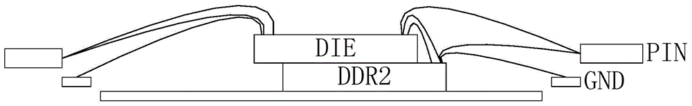
[0023] The same chip design satisfies the eLQFP128 package design of the DDR2 (Second Generation Double Data Rate Synchronous Dynamic Random Access Memory) KGD of two different DRAM manufacturers at the same time. product.

[0024] Since i...


PUM


Abstract

The invention discloses a chip DRAM (dynamic random access memory) pad arrangement structure for improving encapsulation compatibility. The DRAM pads of a chip include a plurality of first pads, a plurality of second pads and a plurality of third pads; the plurality of first pads are arranged at intervals so as to form an inner-row pad group; the plurality of second pads are arranged at intervals so as to form a middle-row pad group; the plurality of third pads are arranged at intervals so as to form an outer-row pad group; the inner-row pad group is located between the center of the chip and the middle-row pad group; the middle-row pad group is located between the inner-row pad group and the outer-row pad group; and the outer-row pad group is located between the middle-row pad group and the boundary of the chip. The chip DRAM pad arrangement structure for improving encapsulation compatibility has the advantages of strong compatibility and no need for encapsulation cost increase, and can satisfy wire bonding requirements of frame-class encapsulation such as WB BGA encapsulation and eLQFP encapsulation.

Description

technical field [0001] The invention relates to the technical field of chip packaging, in particular to a chip DRAM pad arrangement structure for improving packaging compatibility. Background technique [0002] Nowadays, the electronic system market is highly competitive. How to quickly respond to market demand and output lower-cost electronic products has become an important factor in winning the competition. For users, they hope to buy cost-effective products that meet actual needs. For solution providers, being able to provide customized product solutions for high-level, middle-level and low-level user needs will increase sales profits and reduce production and development costs. For an AP (Application Processor, application processor) manufacturer, being able to launch a highly compatible and stable IC (Integrated circuit, integrated circuit) design will be able to shorten the development cycle, reduce design costs, and improve efficiency. [0003] At present, the main...

Claims


Application Information

Patent Timeline
Patent Type & Authority Applications(China)
IPC IPC(8): H01L23/488
CPCH01L24/06H01L2224/05554H01L2224/48091H01L2224/48145H01L2224/49109H01L2924/00014H01L2924/00012
Inventor 陈派林
Owner ALLWINNER TECH CO LTD
Why Eureka
Try Eureka