Preparation methods of silver nanowires for conductive ink and silver nanowire electrode

A silver nanowire and conductive ink technology, applied in the field of printed electronics, can solve the problems of cumbersome preparation process of silver nanomaterials, inability to use large-scale production and application, harsh experimental conditions, etc., and achieve high yield, uniform size, and simple preparation method Effect

Inactive Publication Date: 2015-11-25
TCL CORPORATION
2 Cites 13 Cited by

AI-Extracted Technical Summary

Problems solved by technology

[0004] The purpose of the present invention is to provide a method for preparing silver nanowires for conductive ink, which aims to solve the problems of cumbersome prepa...

Method used

The growth schematic diagram of the silver nanowire described in the embodiment of the present invention 1 is as shown in accompanying drawing 1, specifically, the silver ion in the precursor solution that above-mentioned step S11 prepares obtains, in 140 ℃ of collector type magnetic stirrers During the process of heating and stirring, it is reduced by the EG and slowly nucleates to form silver seeds. The obtained silver seeds include single crystals and polycrystalline seeds with more partial defects or higher defect energy, and some defective parts such as twins and stacking faults are easily etched. Therefore, during the slow heating process, the monocrystalline seed is retained, while the polycrystalline seed is etched by HCl and returns to the solution to form silver ions, which again undergo the reduction by the EG, slow nucleation process. After heating and stirring at 140°C for 2 hours, the silver ions in the precursor solution are screened through multiple cycles of seed crystal formation-polycrystalline etching-seed crystal formation, and basically only the silver ions in the precursor solution remain Single crystal seeds and twin seeds, and most of the seeds grow one-dimensionally along one direction. At this time, it is not enough to realize the growth of one-dimensional silver nanomaterials by prolonging the time. Therefore, after the first heating and stirring treatment, the temperature was increased to 160° C. and heated and stirred to accelerate the one-dimensional growth rate of the reaction seed crystal, and finally obtain standard one-dimensional silver nanowires.
The method that the embodiment of the present invention 1 prepares silver nanowire is simple and controllable, and the product that obtains is the one-dimensional silver nanowire of uniform size; Adopt the flexible electrode that described one-dimensional silver nanowire prepares, has better electrical conductivity , and has a certain degree of curvature, which can be used for flexible printing.
The preparation me...

Abstract

The invention is applicable to the field of printing electronics, and provides preparation methods of silver nanowires for conductive ink and a silver nanowire electrode. The silver nanowires for the conductive ink are prepared by the steps: preparing a precursor solution, and heating and stirring the precursor solution. The silver nanowire electrode can be prepared on a substrate only by dispersing the silver nanowires.

Application Domain

Technology Topic

Silver nanowiresNanotechnology +1

Image

  • Preparation methods of silver nanowires for conductive ink and silver nanowire electrode

Examples

  • Experimental program(2)
  • Comparison scheme(2)

Example Embodiment

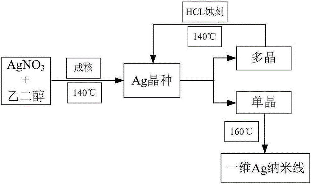
[0018] The embodiment of the present invention provides a method for preparing silver nanowires for conductive ink, including the following steps:
[0019] S01. The silver ion salt and the protective agent are dissolved in a reducing solvent to form a mixed solution, and an etchant is added to the mixed solution to prepare a precursor solution;
[0020] S02. The precursor solution is heated and stirred twice in sequence to prepare silver nanowires for conductive ink, wherein the method of the two heating and stirring treatments is:
[0021] The first heating and stirring treatment: heating and stirring at 135-145℃ for 110-130min;
[0022] The second heating and stirring treatment: heating and stirring at 155-165°C for 25-35 min.
[0023] Specifically, in the above step S01, the mixed solution simultaneously contains a silver ion salt, a protective agent, and a reducing solvent.
[0024] Wherein, the silver ion salt is an organic or inorganic silver ion salt that can exist as a cation in a reducing solution. As a specific preferred embodiment, the silver ion salt includes but is not limited to one of silver nitrate and silver acetate. The reducing solvent can reduce the silver ions in the silver ion salt into elemental silver seed crystals in the following heating and stirring step.
[0025] In order to obtain a better reduction effect without affecting the morphology and yield of the silver nanowires for conductive inks, as a preferred embodiment, the reducing solvent is ethylene glycol, glucose, NaBH 4 , At least one of dimethyl sulfoxide and sodium citrate; more preferably ethylene glycol.
[0026] As another preferred embodiment, the protective agent is at least one of polyvinylpyrrolidone (PVP), sodium lauryl sulfonate, polyvinyl alcohol, and cetyltrimethylammonium bromide; more preferably Polyvinylpyrrolidone.
[0027] In the preparation of the silver nanowires for conductive ink in the embodiment of the present invention, the etching solution is an important factor in controlling the structure and morphology of the silver nanowires for conductive ink. As a preferred embodiment, in the step of adding an etchant to the mixed solution, the volume ratio of the etchant to the mixed solution is (0.95-1.05): (18-22). As another preferred embodiment, the etchant is an acid solution. Specifically, the acid etchant is HCl, H 2 S, HNO 3 At least one of them. Further, the mass fraction of the HCl is preferably 36-38%; the HNO 3 The mass fraction is preferably 64-66%; the H 2 The mass fraction of S is preferably 0.32-0.34%.
[0028] In the above step S02 in the embodiment of the present invention, heating and stirring the precursor solution twice is a key step for preparing the silver nanowires for conductive ink. And the two heating treatment methods are strictly controlled, specifically: the first heating and stirring treatment: heating and stirring at 135-145°C for 110-130 min; the second heating and stirring treatment: at 155-165°C Heat and stir for 25-35min.
[0029] In the first heating and stirring treatment step in the embodiment of the present invention, heating and stirring are carried out at 135-145°C for 110-130 minutes, particularly preferably at 140°C for 120 minutes. The process temperature is relatively low, and the reaction process is slow, in order to allow the seed crystal to grow preferentially and to control the crystal form produced in the solution. At a temperature of 135-145°C, especially 140°C, only a few seed crystals can be produced in the precursor solution, and the growth rate of the seed crystals is slow. At this time, the presence of the etching solution will cause most of the polycrystalline seed crystals in the solution to etch, allowing them to be re-dissolved in the solution. After the etching process of the etching solution, the solution contains polycrystalline seeds with many defects or large defects, and some of the defect sites such as twins and stacking faults are etched. In the embodiment of the present invention, during the first heating and stirring process, the heating and stirring time has a great influence on the morphology of the silver nanowires. Specifically, if the heating and stirring time is not enough, the etching time will be insufficient, resulting in more polycrystalline seed crystals in the solution. These seed crystals will directly develop into spherical nanoparticles in the later growth process. There are a large number of spherical particles. In addition, the growth of these spherical nanoparticles will also consume the "nutrients" for the growth of silver nanowires, so the resulting one-dimensional structure is mostly short rod-shaped silver, not linear silver. After the first long-term heating and stirring treatment, the seed crystals in the solution are screened. At this time, the single crystal seed crystals and a small amount of twin seed crystals in the solution are retained to continue to grow, and most of them have begun to grow along. Expand one-dimensional growth in one direction.
[0030] In the second heating and stirring treatment step in the embodiment of the present invention, heating and stirring are performed at 155-165°C for 25-35 minutes, and particularly preferably, heating and stirring are performed at 160°C for 30 minutes. The relatively high temperature of the process accelerates the reaction process, which is beneficial to the nucleation and rapid growth of single crystal seed crystals and a small amount of twin crystal seed crystals to form a one-dimensional silver nanomaterial with good morphology. In the second heating and stirring treatment step, the heating temperature has a great influence on the structure of the product. Specifically, if the heating temperature is too high, the rapid growth process of the silver nanomaterials is too fast, which causes the seed crystals to grow not only in the horizontal direction, but also in the vertical direction. Therefore, short rod-shaped silver structures appear in the resulting product. A uniform one-dimensional silver nanowire cannot be obtained.
[0031] In the embodiment of the present invention, after the heating and stirring treatment steps, flocculent one-dimensional silver nanowires are obtained in the solution. Further, as a preferred embodiment, it also includes centrifuging the obtained flocculent silver nanowires. The centrifugal treatment method is to perform high-speed centrifugation after diluting the silver nanowires with the flocculent structure. The centrifugal treatment specifically is centrifugation at 7500-8500 rpm for 10-20 min, and the centrifugal treatment is more preferably centrifugation at 8000 rpm for 15 min. Wherein, the dilution treatment may use a solvent that does not dissolve the silver nanowires and does not introduce other impurities. As a specific example, the dilution solvent is an alcohol solvent, such as anhydrous ethanol, anhydrous propanol, and the like.
[0032] In the silver nanowire for conductive ink obtained in the embodiment of the present invention, the diameter of the silver nanowire is 30-40 nm and the length is 8-15 μm. Since the structure of the silver nanowires is relatively complete and the length is relatively long, the silver nanowires can be interwoven into a network. The electrode pattern prepared by printing or spin coating the silver nanowires can directly conduct electricity, and after sintering them, the electrical conductivity will be stronger.
[0033] In the method for preparing silver nanowires for conductive inks provided by the embodiments of the present invention, one-dimensional silver nanowires for conductive inks can be prepared in one step by strictly heating and stirring the precursor solution. The preparation method is simple and the process is controllable. The performance is strong, and the obtained silver nanowire product has uniform size, high yield, good reproducibility, and is easy to realize industrialization.
[0034] And, an embodiment of the present invention also provides a method for preparing a silver nanowire electrode, including the following steps:
[0035] Q01. Prepare silver nanowires for conductive ink according to the above method;
[0036] Q02. Disperse the silver nanowires into a dispersion liquid to form a silver nanowire dispersion system, use the silver nanowire dispersion system on a substrate and sinter to prepare an electrode, wherein the total weight of the dispersion system is 100%, so The mass percentage of the silver nanowires is 20-30%.
[0037] Specifically, in the above step Q01, the method and formula for preparing the silver nanowires for conductive ink have been described in detail above, and in order to save space, the details are not repeated here.
[0038] In the above step Q02, the silver nanowires are dispersed into the dispersion liquid to form a silver nanowire dispersion system, wherein, based on the total weight of the dispersion system as 100%, the weight percentage of the silver nanowires is 20-30 %. When the mass percentage of the silver nanowire is too low, it is difficult to obtain an electrode with excellent conductivity; when the mass percentage of the silver nanowire is too high, the process of preparing the electrode by printing, spin coating, etc. leads to The electrode uniformity is poor, which affects its performance.
[0039] As a preferred embodiment, the dispersion is an alcohol dispersion; the dispersion is more preferably anhydrous ethanol or anhydrous propanol.
[0040] In the embodiment of the present invention, the selection of the substrate can be a rigid substrate or a flexible substrate without limitation. As another preferred embodiment, the substrate is a flexible substrate, and the flexible substrate is one of PI, PEN, and PET. A flexible electrode prepared by using the silver nanowire dispersion system on a substrate and sintering is a flexible electrode with a certain degree of curvature.
[0041] The preparation method of the silver nanowire electrode provided by the embodiment of the present invention is prepared by using the silver nanowire for conductive ink, and the obtained electrode has excellent conductivity, can withstand certain tortuosity, and is suitable for flexible printing.

Example Embodiment

[0043] Example 1
[0044] A method for preparing a flexible electrode includes the following steps:
[0045] Q11. The preparation of silver nanowires for conductive inks includes the following steps:
[0046] S11. Put 100mgAgNO 3 Dissolve 100mg PVP in 30ml EG, add 2ul HCl (1M) to it after dissolving evenly to prepare a precursor solution;
[0047] S12. Pour the precursor solution into a flask and perform heating and stirring treatment twice in turn,
[0048] Among them, the first heating and stirring treatment is placed in a heat-collecting magnetic stirrer at 140°C for 2 hours, and the reaction equation of the first heating and stirring treatment is as follows:
[0049] 2HOCH 2 CH 2 OH→2CH 3 CHO+2H 2 O(S121)
[0050] 2Ag + +2CH 3 CHO→CH 3 CHO-OHCCH 3 +2Ag+2H + (S122)
[0051] 4HNO 3 +3Ag→3AgNO 3 +NO+2H 2 O(S123),
[0052] Among them, the reaction formula S123 reflects the reaction process of the polycrystalline crystal nucleus being etched.
[0053] For the second heating and stirring treatment, increase the temperature to 160°C, and heat and stir for 30 minutes,
[0054] The schematic diagram of the growth of the silver nanowires described in Example 1 of the present invention is as attached figure 1 As shown, specifically, the silver ions in the precursor solution prepared in the above step S11 are reduced by the EG during heating and stirring in a heat-collecting magnetic stirrer at 140° C., and slowly nucleate to form silver seeds. The obtained silver seed crystals include single crystals and polycrystalline seed crystals with a large number of defects or large defect energy, some of which are easily etched, such as twins and stacking faults. Therefore, during the slow heating process, the single-crystal seed crystals are retained, while the poly-crystal seed crystals are etched by HCl and return to the solution to form silver ions, which are reduced and slowly nucleated by the EG. process. After heating and stirring for 2 hours at 140°C, the silver ions in the precursor solution have been screened for multiple cycles of seed crystal formation-polycrystalline etching-seed crystal formation, and basically only left in the precursor solution Single crystal seed crystals and twin crystal seed crystals, and most of the seed crystals grow one-dimensionally along one direction. At this time, the growth of one-dimensional silver nanomaterials can no longer be satisfied by extending the time. Therefore, after the first heating and stirring treatment, the temperature is increased to 160° C. and heating and stirring to accelerate the one-dimensional growth rate of the reaction seed crystal, and finally obtain standard one-dimensional silver nanowires.
[0055] S13. After the above heating process is over, take out the flask and let it cool naturally at room temperature; add absolute ethanol to the cooled product to dilute it by equal volume 2 times, and then centrifuge at 8000 rpm for 15 min in a high-speed centrifuge. Pour the upper clear liquid containing reaction residues and impurities, and repeat the centrifugation treatment 2 to 3 times.
[0056] Q12. Disperse the separated silver nanowires in absolute ethanol at a ratio of 25 wt%, prepare them on a cleaned flexible substrate by printing or spin coating, and sinter to obtain a flexible electrode with a certain degree of curvature.
[0057] The method for preparing silver nanowires in Example 1 of the present invention is simple and controllable, and the product obtained is a one-dimensional silver nanowire of uniform size; the flexible electrode prepared by using the one-dimensional silver nanowire has good electrical conductivity and has A certain degree of curvature can be used for flexible printing.

PUM

PropertyMeasurementUnit
Diameter30.0 ~ 40.0nm
Length8.0 ~ 15.0µm
tensileMPa
Particle sizePa
strength10

Description & Claims & Application Information

We can also present the details of the Description, Claims and Application information to help users get a comprehensive understanding of the technical details of the patent, such as background art, summary of invention, brief description of drawings, description of embodiments, and other original content. On the other hand, users can also determine the specific scope of protection of the technology through the list of claims; as well as understand the changes in the life cycle of the technology with the presentation of the patent timeline. Login to view more.

Similar technology patents

Classification and recommendation of technical efficacy words

  • Strong process controllability
  • Easy to prepare

Method for controlling growing multiple layer film for making multiple-level micro-reflector

Owner:CHANGCHUN INST OF OPTICS FINE MECHANICS & PHYSICS CHINESE ACAD OF SCI
Why Eureka
Try Eureka