Formation method of semiconductor structure

A semiconductor and gate structure technology, which is applied in the field of semiconductor structure formation, can solve the problems such as the performance of MOS transistors needs to be improved, and achieve the effects of preventing bridging phenomenon, increasing the window, and improving integration

Active Publication Date: 2015-11-25
SEMICON MFG INT (SHANGHAI) CORP
View PDF4 Cites 14 Cited by
  • Summary
  • Abstract
  • Description
  • Claims
  • Application Information

AI Technical Summary

Problems solved by technology

[0004] However, the performance of MOS transistors f...

Method used


Image

  • Formation method of semiconductor structure
  • Formation method of semiconductor structure
  • Formation method of semiconductor structure

Examples


Embodiment Construction

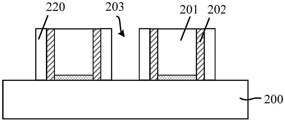
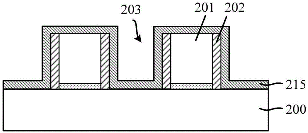
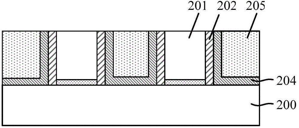
[0031]In the prior art, in the process of forming metal plugs connecting the source / drain regions, after forming the first dielectric layer, it is necessary to form a photoresist layer with openings on the first dielectric layer, and then use the photoresist layer as a mask, etch the first dielectric layer to form etching holes in the first dielectric layer, but as the integration of devices continues to increase, the distance between adjacent gate structures is also getting smaller and smaller, which means It is required that the size of the opening formed in the photoresist layer is also continuously reduced, and is limited by the photolithography equipment and process conditions. When the size of the opening formed in the photoresist layer is very small (less than 80 nanometers), it can be developed by exposure The opening formed in the photoresist layer by the process is prone to shift in position, so that the position of the etching hole formed by etching the first dielect...


PUM

PropertyMeasurementUnit
Thicknessaaaaaaaaaa
Thicknessaaaaaaaaaa

Abstract

A formation method of a semiconductor structure comprises the steps of providing a semiconductor substrate, wherein a plurality of grid structures are formed on the semiconductor substrate, first openings are formed between the adjacent grid structures, source/drain regions are formed at the two sides of the grid structures, and etching stop layers are arranged on the surfaces of the grid structures; forming first dielectric layers in the first openings, wherein the surfaces of the first dielectric layers are lower than the top surfaces of the grid structures; forming size adjusting material layers covering the surfaces of the first dielectric layers and the grid structures; using a markless etching technology to etch the size adjusting material layers, and forming size adjusting side walls on the surfaces of the side walls of the etching stop layers; forming second dielectric layers covering the grid structures and the size adjusting side walls; etching the second dielectric layers, and forming second openings in the second dielectric layers, wherein the second openings expose out of the size adjusting side walls; etching the first dielectric layers in the first openings and the etching stop layers to form third openings. By forming the size adjusting side walls, a photoetching technology window is enlarged, and a bridging phenomenon is prevented.

Description

technical field [0001] The invention relates to the field of semiconductor manufacturing, in particular to a method for forming a semiconductor structure. Background technique [0002] Metal-oxide-semiconductor (MOS) transistors are the most basic devices in semiconductor manufacturing. They are widely used in various integrated circuits. According to the main carrier and the type of doping during manufacturing, they are divided into NMOS and PMOS transistors. [0003] The prior art provides a method for manufacturing a MOS transistor, including: providing a semiconductor substrate, forming a gate structure on the semiconductor substrate, the gate structure including a gate dielectric layer and a gate electrode located on the gate dielectric layer ; forming offset sidewalls on the sidewall surfaces on both sides of the gate structure; using the gate structure and the offset sidewalls as a mask, performing shallow dopant ion implantation, and semiconductor substrates on both ...

Claims


Application Information

Patent Timeline
IPC IPC(8): H01L21/768H01L21/336
Inventor 王新鹏
Owner SEMICON MFG INT (SHANGHAI) CORP
Why Eureka
Try Eureka