Integrated circuit test system and method
A technology of integrated circuits and test systems, which is applied in the direction of measuring electricity, measuring devices, measuring electrical variables, etc., can solve the problems of high cost and low test rate, and achieve the effect of reducing test cost, improving test efficiency, and overcoming low efficiency.
- Summary
- Abstract
- Description
- Claims
- Application Information
AI Technical Summary
Problems solved by technology
Method used
Image

Examples
Embodiment 1
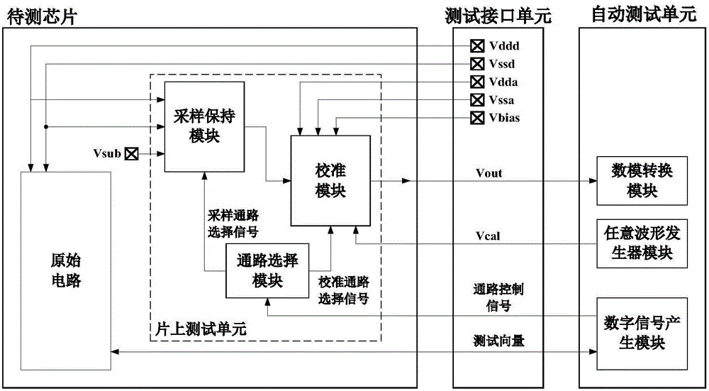
[0032] image 3 It is a schematic block diagram of the structure of the integrated circuit testing system in Embodiment 1 of the present invention.
[0033] Such as image 3 As shown, the chip under test refers to the integrated circuit chip to be tested. In the present invention, it is the object under test, and its power supply noise signal needs to be measured. The integrated circuit test system of the present invention comprises a chip to be tested, an automatic test unit and a test interface unit, the chip to be tested and the automatic test unit are connected through the test interface unit, in order to achieve the purpose of the present invention, in the chip to be tested, in addition In addition to the original circuit to realize the original function of the chip, an on-chip test unit needs to be embedded on the chip. The on-chip test unit includes: sample and hold module, calibration module and channel selection module.
[0034] In order to improve test efficiency a...
Embodiment 2
[0041] Figure 4 It is a schematic block diagram of the structure of the integrated circuit testing system in Embodiment 2 of the present invention.
[0042] Such as Figure 4 As shown, the test system includes a chip to be tested, an on-chip test unit, a test interface board and an integrated circuit automatic test equipment (ATE).
[0043] In Embodiment 2, the test interface unit can be a test interface board, and the chip to be tested is installed on the test interface board through a test socket, including a ball grid array package (BGA) package socket, a quad flat package (QFP) package socket, etc. The test interface board provides Vddd, Vssd, Vdda, Vssa, Vbias and other signals for the chip under test ( Figure 5 And the corresponding text description below will give a detailed explanation of the signals represented by these letters) supply voltage, and forward the Vcal, channel control signal, test vector and other signals output by the automatic test unit to the chip u...
Embodiment 1 and 2
[0054] Utilize embodiment 1 and 2 and other embodiments of the present invention:
[0055] (1) It can realize the test of high-speed chips
[0056] Since the present invention applies test vectors to the chip to be tested by an automatic test unit such as ATE, checks the correctness of the output response signal of the chip to be tested, and uses the on-chip test unit to complete the sampling and holding of the bypass signal, and utilizes the internal analog-to-digital conversion of the ATE Module to complete the digitization of the bypass signal, so it can realize the test of the high-speed (such as GHz) chip under test, thereby improving the test efficiency and reducing the test cost;
[0057] (2) It can be integrated with the existing integrated circuit test process
[0058] Existing integrated circuit testing processes are all carried out using ATE, and the embodiment of the present invention does not need to carry out additional technical transformation on ATE, and only ...
PUM
 Abstract
Description
Claims
Application Information
 - R&D
- Intellectual Property
- Life Sciences
- Materials
- Tech Scout
- Unparalleled Data Quality
- Higher Quality Content
- 60% Fewer Hallucinations
Browse by: Latest US Patents, China's latest patents, Technical Efficacy Thesaurus, Application Domain, Technology Topic, Popular Technical Reports.
© 2025 PatSnap. All rights reserved.Legal|Privacy policy|Modern Slavery Act Transparency Statement|Sitemap|About US| Contact US: help@patsnap.com