Method for designing focus-length-controllable and one-dimensional photonic crystal flat concave mirror

A dimensional photonic crystal and design method technology, applied in the direction of light guides, optics, optical components, etc., can solve the problems that can only be realized near the lens surface, cannot propagate a long distance, and is difficult to achieve effective applications, etc., to shorten the design Cycle, simple design method, easy-to-manufacture effect

Active Publication Date: 2015-12-02
NANJING UNIV OF POSTS & TELECOMM
4 Cites 10 Cited by

AI-Extracted Technical Summary

Problems solved by technology

GiladM.Lerman and others experimentally verified the focusing of radially polarized light by the plasmonic lens in the article entitled "Demonstration of Nanofocusing by the use of PlasmonicLens Illuminated with Radially Polarized Light", see NANOLETTERS Volume 9, Issue 5, Page 2139-2143, but the plasmonic lens The plasmon is a coupling mode of the evanescent wave, which cannot propagate for a long distance, and can only focus near the lens surfa...

Abstract

The invention discloses a method for designing a focus-length-controllable and one-dimensional photonic crystal flat concave mirror. The one-dimensional photonic crystal flat concave mirror is composed of one-dimensional photonic crystals formed through the alternate arrangement of a material A and a material B. Circular rings of fixed thickness are stacked up to form the one-dimensional photonic crystal flat concave mirror, wherein the structural parameters of photonic crystals are adopted as one unit of the circular rings and the internal diameters of the circular rings are gradually increased from bottom to top. The emitting surface of the one-dimensional photonic crystal flat concave mirror is in the form of a recessed surface formed through connecting the upper edges of adjacent circular rings. According to the technical scheme of the invention, the flat concave mirror is controllable in focus length. In this way, the structural parameters of a flat concave mirror of any focal length within a certain range can be automatically designed, and the incident ray and the emergent ray are positioned at the two ends of the incident plane of the flat concave mirror. Meanwhile, the method has no special requirement on the polarization state of the incident ray, and breaks through the dependency on the polarization of surface plasmon lens. Moreover, the light focusing in both the TE polarization state and the TM polarization state is realized at the same time. The method is also applicable to linearly polarized lights. The invention has the advantages of simple design method and simple manufacture. By adopting the design method, the design cycle is shortened.

Application Domain

Technology Topic

Design cycleConcave surface +9

Image

  • Method for designing focus-length-controllable and one-dimensional photonic crystal flat concave mirror
  • Method for designing focus-length-controllable and one-dimensional photonic crystal flat concave mirror
  • Method for designing focus-length-controllable and one-dimensional photonic crystal flat concave mirror

Examples

  • Experimental program(1)

Example Embodiment

[0024] The present invention will be further described below in conjunction with the drawings and specific embodiments.
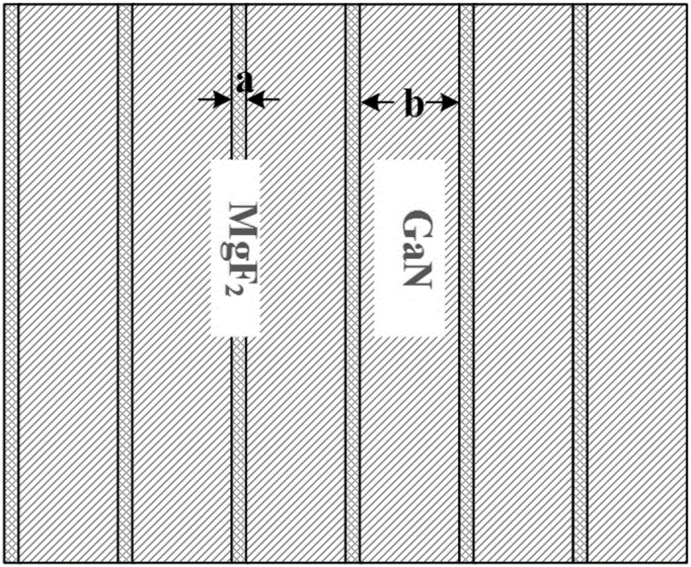
[0025] Design a one-dimensional photonic crystal plano-concave lens with a controllable focal length. The plano-concave lens is composed of one-dimensional photonic crystals with two materials A and B alternately arranged. The structural parameters of the photonic crystal are used as the unit, the thickness is fixed, and the inner diameter is from bottom to top. Increasing rings are laminated, and the exit surface is a concave surface connected along the adjacent ring layers, and the focal length is 6.5 μm in the visible light band.
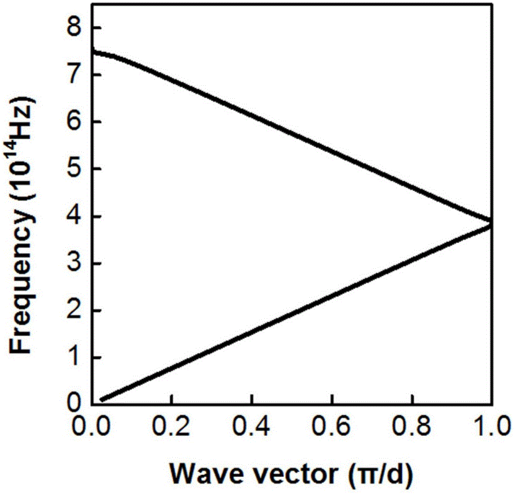
[0026] First, determine that the light wave band of the plano-concave mirror is in the visible light band. After calculating the dispersion relationship of the one-dimensional photonic crystal, two materials MgF are selected. 2 And GaN, the refractive indices of the two are 1.38 and 2.67, and the thickness is a=10nm and b=140nm, see figure 1.
[0027] Calculate MgF 2 The negative refraction bands alternately arranged when the thickness of GaN and GaN are 10nm and 140nm respectively, which are located in the band 3.9×10 14 Hz to 7.5×10 14 Hz, the band is in the visible light 3.9474×10 14 Hz to 7.8947×10 14 Within the Hz band, meet the design requirements, see figure 2.
[0028] Use equal frequency curve combined with the law of refraction to calculate the equivalent negative refractive index. in image 3 Among them, the circle represents the equal frequency curve of light with a wavelength of 532nm propagating in the air, and the remaining lines represent the equal frequency curve of light with a wavelength of 532nm propagating in the photonic crystal under TE and TM polarization states, marked α i With α r The size of is equal to the incident angle and the exit angle at both ends of the exit surface. After calculating the equal frequency curve, the edge AC=0.2668 can be obtained. For a one-dimensional photonic crystal with a specific structure at a specific frequency, the AC edge is a fixed value. The radius R of the circle represents the size of the wave vector in the air, so the side BC=R=d/λ=150/532=0.2820, the calculation here takes into account the unit of 2π/d in the figure. In △ABC, ∠A=α i , ∠B=-α r Then there are:
[0029] n T E = n T M = - s i n ∠ B sin ∠ A = - A C B C = - 0.2658 0.2820 = - 0.94
[0030] Then the equivalent negative refractive index of the one-dimensional photonic crystal is -0.94.
[0031] Calculate the topography parameters of the plano-concave lens: the exit surface of the plano-concave lens with cylindrical symmetrical structure is a bare period, viewed from the cross section along the axial direction, the exit surface is composed of the lines of the tips of adjacent periods. Small triangle, let the focal point f=6.5μm, the equivalent negative refractive index has been calculated as n=-0.94, by Figure 4 It can be seen that the initial value x 0 =0, the coordinates of the tip of each layer of bare photonic crystal corresponding to the concave side of the entire plano-concave mirror can be calculated by using the following equations:
[0032] t a n ( α i ) = d x k - x k - 1 ( 1 ) t a n ( α i + | α | ) = x k + x k - 1 2 f - 2 k - 1 2 d ( 2 ) n = sin ( α r ) sin ( α i ) ( 3 ) d = a + b ( 4 )
[0033] Calculated x k The values ​​are shown in Table 1:
[0034] Table 1 Corresponding concave surface profile data when the focal length is 6.5μm (unit: μm)
[0035] x0
[0036] Figure 5 , To verify the accuracy of the designed plano-concave mirror. The focusing effect of the plano-concave mirror structure obtained by Table1 on radially polarized light is as follows Figure 5 As shown in (a), the wavelength of the incident light is 532nm, and the electric field amplitude distribution in the radial and rotational directions of the incident light is approximated by Bessel-Gauss distribution Figure 5 (b) The normalized energy distribution along the z-axis is given, showing that the simulation results are consistent with the theoretical calculations.
[0037] Image 6 The electric field distribution diagram of a one-dimensional photonic crystal plano-concave mirror with a focal length of 7.5 μm is also given ( Image 6 a) and the normalized energy distribution along the z axis ( Image 6 b). This shows that the equations in this design method can be used to characterize the constitutive parameters of the structure, and then be applied to design plano-concave mirrors with controllable focal length.
[0038] As described above, although the present invention has been shown and described with reference to specific embodiments, it should not be construed as limiting the present invention itself. Various changes can be made in the form and details of the method of the present invention as defined by the appended claims.

PUM

no PUM

Description & Claims & Application Information

We can also present the details of the Description, Claims and Application information to help users get a comprehensive understanding of the technical details of the patent, such as background art, summary of invention, brief description of drawings, description of embodiments, and other original content. On the other hand, users can also determine the specific scope of protection of the technology through the list of claims; as well as understand the changes in the life cycle of the technology with the presentation of the patent timeline. Login to view more.

Similar technology patents

Adjustable LCL filter optimization design method of T-type three-level energy storage converter

PendingCN114070025AImprove the quality of grid-connected powerSimple design methodAc-dc conversionDesign optimisation/simulationCapacitanceComplex filter
Owner:SHANDONG ELECTRICAL ENG & EQUIP GRP +1

Classification and recommendation of technical efficacy words

  • Easy to manufacture
  • Simple design method

Methylation high-flux detection method

ActiveCN102796808AThe data is true and sufficientSimple design methodMicrobiological testing/measurementLibrary creationBioinformaticsBisulfite sequencing
Owner:BGI TECH SOLUTIONS

Ultra-wideband filter based on simplified left hand transmission line structure

InactiveCN101246983ASimple design methodIn-band insertion loss is smallWaveguide type devicesTransmission lineShunt capacitance
Owner:NANJING UNIV
Why Eureka
Try Eureka