
Method of preparing various single-side multilayer single-functional and single-side and double-side multilayer multifunctional printed electronic product by virtue of light induction
An electronic product, light-induced technology, applied in the direction of electric recording technology, printed circuit, conductive pattern formation, etc., which can solve the problems of high efficiency, high resolution, and large-scale electronic circuit production, and achieve green Environmentally friendly and efficient production, no waste liquid, and small investment in equipment
- Summary
- Abstract
- Description
- Claims
- Application Information
AI Technical Summary
Problems solved by technology
Method used
Image

Examples
specific Embodiment approach 1
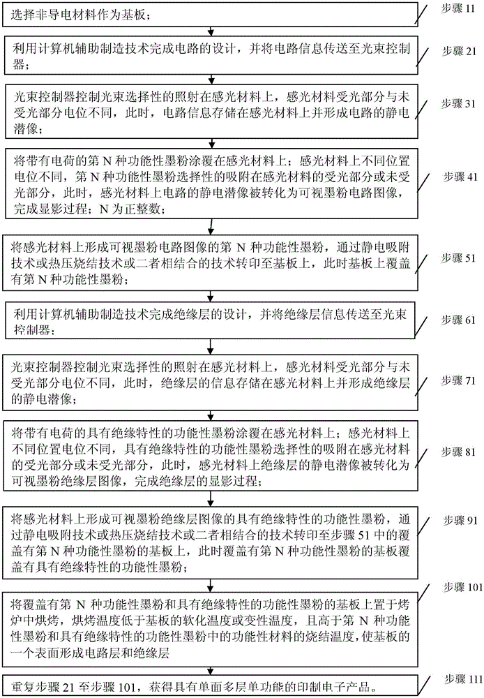
[0039] Specific implementation mode 1, refer to figure 1 Specifically explain this embodiment, the method for preparing a single-sided multi-layer single-function printed electronic product using light induction described in this embodiment, it includes the following steps:
[0040] Step 11, selecting a non-conductive material as the substrate;
[0041] Step 21, using computer-aided manufacturing technology to complete the design of the circuit, and sending the circuit information to the beam controller;
[0042] Step 31, the light beam controller controls the light beam to selectively irradiate the photosensitive material, and the potential of the light-receiving part of the photosensitive material is different from that of the non-light-receiving part. At this time, the circuit information is stored on the photosensitive material and forms an electrostatic latent image of the circuit;
[0043]Step 41, coating the Nth functional toner with charge on the photosensitive materi...
specific Embodiment approach 2
[0054] Embodiment 2. Based on Embodiment 1, the method for preparing a double-sided multilayer single-function printed electronic product includes the following steps:
[0055] Step 1-1, selecting a non-conductive material as the substrate;
[0056] Step 2-1, using computer-aided manufacturing technology to complete the design of the circuit, and sending the circuit information to the beam controller;
[0057] Step 3-1, the light beam controller controls the light beam to selectively irradiate the photosensitive material, and the potential of the light-receiving part of the photosensitive material is different from that of the non-light-receiving part. At this time, the circuit information is stored on the photosensitive material and forms an electrostatic latent image of the circuit;
[0058] Step 4-1, coating the Nth functional toner with charge on the photosensitive material; different positions on the photosensitive material have different potentials, and the Nth functiona...
specific Embodiment approach 3
[0068] Specific Embodiment Three. The method for preparing a single-sided multi-layer single-function printed electronic product using light induction described in this embodiment includes the following steps:
[0069] Step A, selecting a non-conductive material as the substrate;
[0070] Step B, using computer-aided manufacturing technology to complete the design of the circuit, and sending the circuit information to the beam controller;
[0071] Step C, the light beam controller controls the light beam to selectively irradiate the photosensitive material, and the potential of the light-receiving part of the photosensitive material is different from that of the non-light-receiving part. At this time, the circuit information is stored on the photosensitive material and forms an electrostatic latent image of the circuit;
[0072] Step D, coating the Nth functional toner with charge on the photosensitive material; different positions on the photosensitive material have different...
PUM
 Abstract
Description
Claims
Application Information