
Flexible substrate, preparation method thereof, and display device

A flexible substrate and flexible display technology, which is applied in semiconductor/solid-state device manufacturing, electrical components, electric solid-state devices, etc., can solve the problems of affecting the manufacturing process, increasing the off-state current, and unable to planarize the functional layer, so as to prevent adverse effects, The effect of preventing carbonization by heat

Inactive Publication Date: 2015-12-02
BOE TECH GRP CO LTD
View PDF5 Cites 20 Cited by
  • Summary
  • Abstract
  • Description
  • Claims
  • Application Information

AI Technical Summary

Problems solved by technology

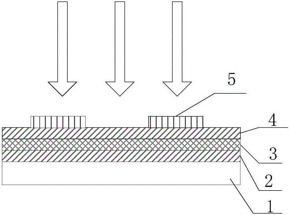
[0003] In this process, the crystallization of low-temperature polysilicon is often carried out by excimer laser annealing (ELA). During the laser action, a-si absorbs laser energy, crystallizes, and becomes p-si, but some The laser energy will reach the flexible substrate and make it carbonized, for example, produce fine particles, cracks, etc., which will make the functional layer of the subsequent process unable to be flattened, affecting the subsequent process
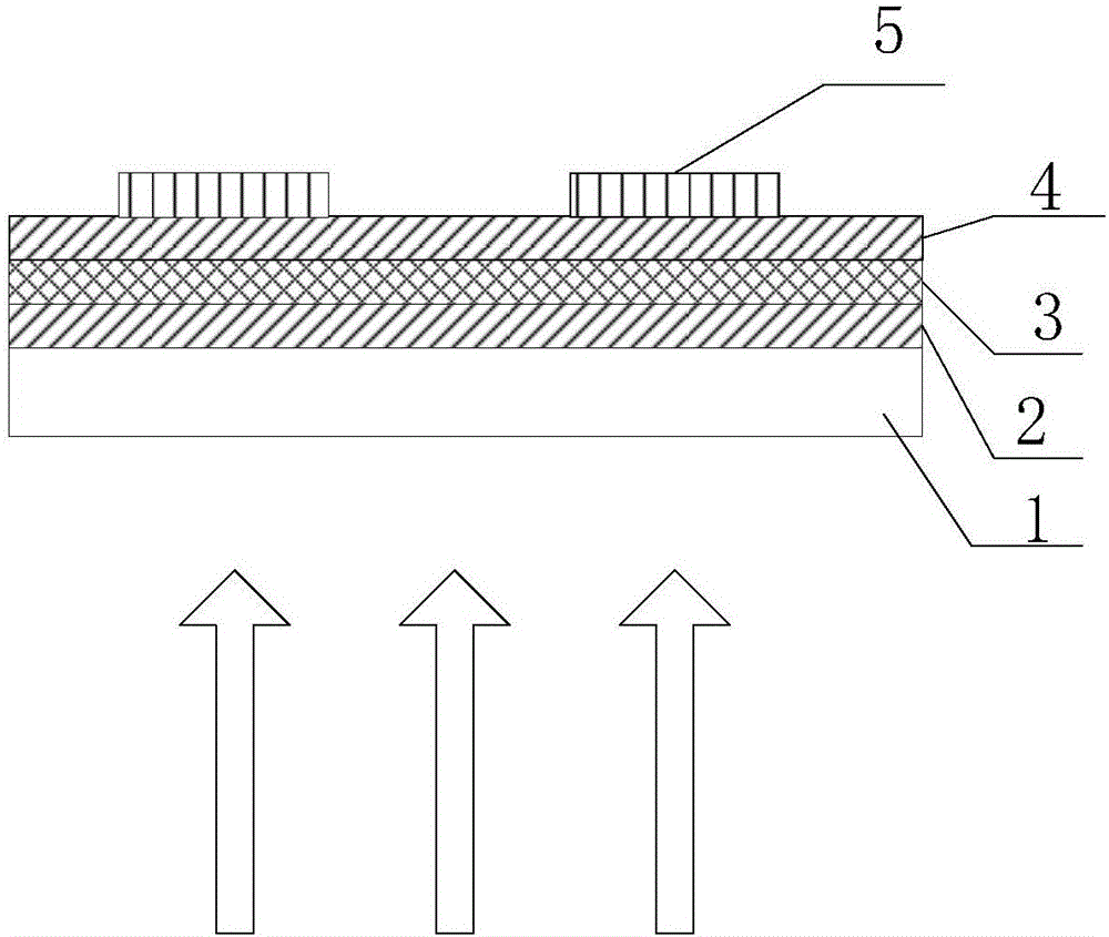
[0004] In addition, after the flexible display device is completed, the flexible display device is generally separated from the glass substrate by means of laser lift-off. Specifically, when the laser is incident on the side of the flexible display device away from the glass substrate, most of the energy irradiated by the laser is instantaneous. Absorbed by the flexible substrate, separation occurs between the flexible substrate and the glass substrate; but the instantaneous high heat will be transferred to the thin film transistor on the flexible substrate, which will affect the characteristics of the thin film transistor, for example, the threshold voltage of the thin film transistor will drift , the off-state current increases, and the switching ratio becomes larger, which deteriorates the characteristics of the thin film transistor and affects its driving ability

Method used


Image

  • Flexible substrate, preparation method thereof, and display device
  • Flexible substrate, preparation method thereof, and display device
  • Flexible substrate, preparation method thereof, and display device

Examples


Embodiment 1

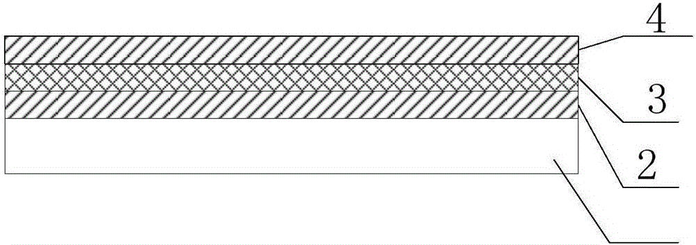
[0031] Such as figure 1 As shown, this embodiment provides a flexible substrate, including a first flexible layer and a second flexible layer 4, and an ultraviolet light absorbing layer 3 disposed between the first flexible layer 2 and the second flexible layer 4 , wherein, the absorption capacity of the ultraviolet light absorbing layer 3 to ultraviolet light is greater than or equal to the absorption capacity of the first flexible layer 2 and the second flexible layer 4 to ultraviolet light.

[0032] In the flexible substrate and its preparation method and display device provided by the present invention, since the flexible substrate includes an ultraviolet light absorbing layer 3 arranged between two flexible layers, the ultraviolet light absorbing layer 3 can be irradiated with an excimer laser on the active layer When converting amorphous silicon to polysilicon, the flexible substrate with a sandwich ultraviolet absorbing layer 3 can absorb excess laser energy by using th...

Embodiment 2

[0040] This embodiment provides a method for preparing the above-mentioned flexible substrate, comprising the following steps:

[0041] forming a first flexible layer 2 on the substrate;

[0042] forming an ultraviolet light absorbing layer 3 on the first flexible layer 2;

[0043] A second flexible layer 4 is formed on the ultraviolet light absorbing layer 3 .

[0044] specifically,

[0045] S1-1, forming a first polyimide layer on the glass substrate 1;

[0046] The specific preparation method is in the scope of the prior art and will not be repeated here. For example, the coating method can be used to control the thickness of the coating film layer, and the first polyimide film with a thickness of 5-30 microns can be formed according to the specific application situation. amine layer.

[0047] S1-2, forming an amorphous silicon layer on the first flexible layer 2;

[0048] Specifically, the a-si film layer can be deposited on the first polyimide layer by plasma vapor d...

Embodiment 3

[0053] This embodiment provides a flexible display device and a manufacturing method thereof, wherein the flexible display device includes the above-mentioned flexible substrate and a thin film transistor disposed on the flexible substrate, and an active layer of the thin film transistor includes a polysilicon layer.

[0054] The preparation method of the flexible display device comprises the following steps:

[0055] Prepare a flexible substrate;

[0056] Fabricating a thin film transistor including a polysilicon active layer on a flexible substrate;

[0057] The flexible display device is separated from the substrate.

[0058] specifically,

[0059] S2-1, preparing a flexible substrate;

[0060] For the preparation method of the flexible substrate, see S1-1 to S1-3 in Example 2;

[0061] S2-2 Preparation of a thin film transistor including a polysilicon active layer on a flexible substrate

[0062] Such as figure 2 As shown, a thin film transistor including a polysilico...


PUM

PropertyMeasurementUnit
Wavelengthaaaaaaaaaa
Thicknessaaaaaaaaaa
Thicknessaaaaaaaaaa

Abstract

The invention provides a flexible substrate, a preparation method thereof, a flexible display device, a preparation method thereof, a display substrate, and a display device in order to solve a problem that in a flexible device manufacture process in the prior art, laser energy has an adverse effect on the polycrystalline silicon active layer of a thin-film transistor and is liable to cause flexible layer carbonization in a flexible display device stripping process. The flexible substrate comprises an ultraviolet light absorption layer arranged between two flexible layers. When the active layer converts amorphous silicon into polycrystalline silicon by means of excimer laser irradiation, the flexible substrate with the sandwiched ultraviolet light absorption layer may absorb redundant laser energy by means of the ultraviolet light absorption layer in order to prevent the flexible layers from being heated and carbonized. When the flexible substrate and a glass substrate are separated, a stripping laser beam is injected from the glass substrate and the flexible substrate may absorb redundant laser energy by means of the ultraviolet light absorption layer in order to prevent the laser beam from having an adverse effect on the performance of the active layer.

Description

technical field [0001] The present invention relates to the field of display technology, in particular to a flexible substrate and a preparation method thereof, a flexible display device and a preparation method thereof, a display substrate, a display panel, and a display device. Background technique [0002] The preparation method of flexible display devices is usually to coat a flexible substrate on a glass substrate, and then prepare low-temperature polysilicon thin-film transistors and light-emitting elements on the flexible substrate. The flexible device is separated from the glass substrate, and finally a flexible display device is obtained. [0003] In this process, the crystallization of low-temperature polysilicon is often carried out by excimer laser annealing (ELA). During the laser action, a-si absorbs laser energy, crystallizes, and becomes p-si, but some The laser energy will reach the flexible substrate and make it carbonized, for example, produce fine partic...

Claims


Application Information

Patent Timeline
IPC IPC(8): H01L27/12H01L21/683
Inventor 谢春燕谢明哲
Owner BOE TECH GRP CO LTD
Learn More