A vertical tunneling field effect transistor

A tunneling field effect and transistor technology, applied in semiconductor devices, electrical components, circuits, etc., can solve the problems of increasing static power consumption of devices and increasing leakage current, reducing leakage current, increasing on-state current, The effect of reducing the tunneling distance

Active Publication Date: 2015-12-02
UNIV OF ELECTRONICS SCI & TECH OF CHINA
View PDF4 Cites 7 Cited by
  • Summary
  • Abstract
  • Description
  • Claims
  • Application Information

AI Technical Summary

Problems solved by technology

However, the narrow bandgap material also inevitably increases the lea

Method used


Image

  • A vertical tunneling field effect transistor
  • A vertical tunneling field effect transistor
  • A vertical tunneling field effect transistor

Examples


Embodiment

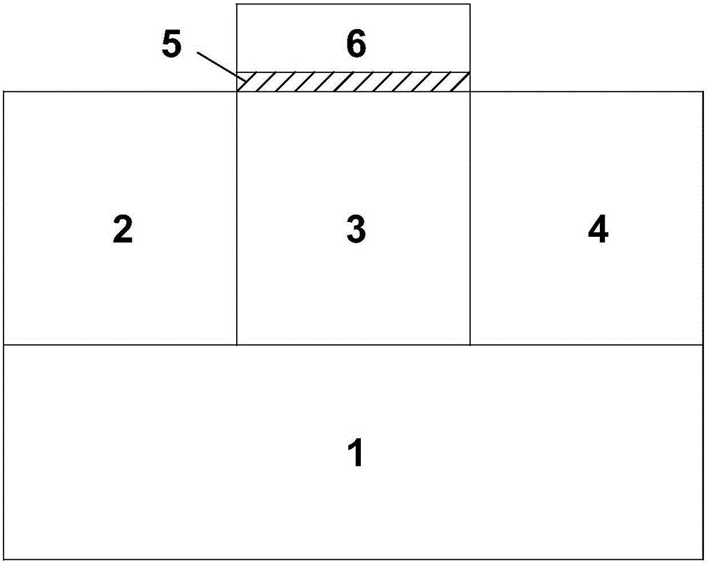
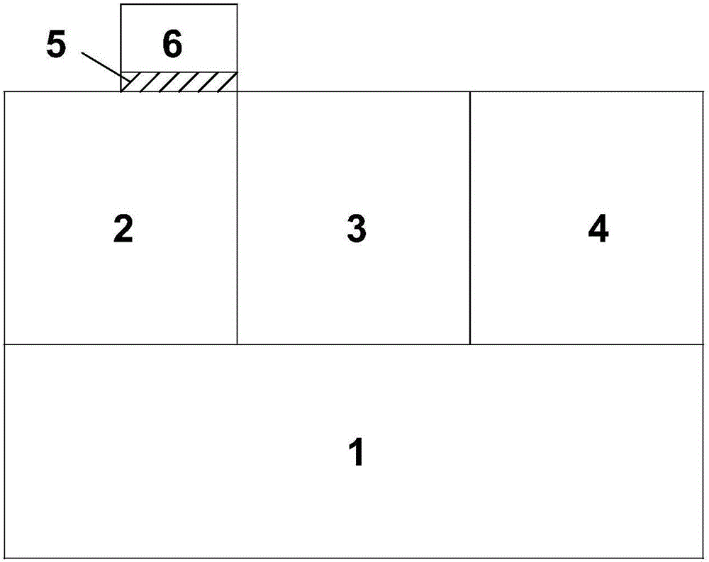
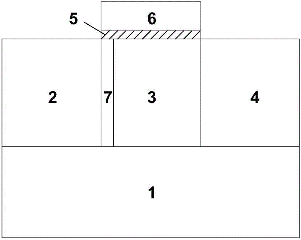
[0033] For the longitudinal tunneling field effect transistor in the embodiment of the present invention, the cross-sectional view of the device can be found in Figure 5 , which includes a semiconductor substrate 1, a source region 2, an intrinsic region 3, a drain region 4, a gate oxide layer 5, a metal gate 6, a buffer layer 10, an epitaxial intrinsic region 11, a stress film 12 and two sidewalls 9, Wherein, the buffer layer 10 is disposed above the semiconductor substrate 1, the source region 2, the intrinsic region 3 and the drain region 4 are respectively disposed above the buffer layer 10, and the two sides of the intrinsic region 3 are connected to the source region 2 and the drain region 4 respectively. The source region 2 and the intrinsic region 3 have the same thickness and are smaller than the thickness of the drain region 4. The epitaxial intrinsic region 11 is arranged above the intrinsic region 3, one side is in contact with the drain region 4, and the other sid...


PUM

PropertyMeasurementUnit
Thicknessaaaaaaaaaa

Abstract

The invention relates to semiconductor technology. The invention provides a vertical tunneling field effect transistor which can increases device on-state currents while not increasing device leakage currents. Technical scheme is summarized in that as for the vertical tunneling field effect transistor, a buffer layer is arranged above a semiconductor substrate; a source region, an intrinsic region and a leakage region are respectively arranged above the buffer layer; an epitaxial intrinsic region is arranged above the intrinsic region; one side of the epitaxial intrinsic region is in contact with the leakage region, and the opposite side of the epitaxial intrinsic region extends to be above one portion of the source region; a gate oxide layer is arranged above the portion where the source region overlaps with the epitaxial intrinsic region; a metal gate is arranged above the gate oxide layer; one side wall is arranged above the source region and the other side wall is arranged above the epitaxial intrinsic region and the leakage region; a stress film covers the source region, the leakage region, the metal gate and the two side walls. The beneficial effects of the vertical tunneling field effect transistor of the present invention are that; a buried oxide layer is provided with an opening below a drain electrode; the device on-state currents can be increased while the device leakage currents are not increased; and the invention is applicable to tunneling field effect transistors.

Description

technical field [0001] The present invention relates to semiconductor technology, and in particular to tunneling field effect transistors (TFETs). Background technique [0002] Since the invention of silicon-based microelectronics, silicon-based microelectronics technology has been based on proportionally reducing the feature size as the main means, and it has developed according to Moore's law. As feature sizes continue to shrink, negative effects such as device short-channel effects are increasing. DIBL (drain-to-barrier-lowering effect) and band-to-band tunneling effect make the off-state leakage current of the device continuously increase. Not only that, the sub-threshold swing of traditional MOSFET devices cannot be reduced synchronously with the reduction of device size due to the theoretical limitation of KT / q. Therefore, the sub-threshold leakage current is also increasing along with the reduction of device threshold voltage. Today, the resulting static power consu...

Claims


Application Information

Patent Timeline
IPC IPC(8): H01L29/739H01L29/06
CPCH01L29/0607H01L29/7391
Inventor 王向展刘葳曹建强
Owner UNIV OF ELECTRONICS SCI & TECH OF CHINA
Why Eureka
Try Eureka