High-response avalanche photodiode fabrication method

An avalanche photoelectric and diode technology, which is applied in the direction of circuits, electrical components, semiconductor devices, etc., can solve the problems of process complexity and high growth cost, and achieve the effect of increasing the light absorption length and reducing the preparation cost

Inactive Publication Date: 2015-12-02
INST OF SEMICONDUCTORS - CHINESE ACAD OF SCI
View PDF4 Cites 15 Cited by
  • Summary
  • Abstract
  • Description
  • Claims
  • Application Information

AI Technical Summary

Problems solved by technology

However, due to the complexity of its process, not only the growth cost is high, but also each step needs to be precisely controlled

Method used


Image

  • High-response avalanche photodiode fabrication method
  • High-response avalanche photodiode fabrication method
  • High-response avalanche photodiode fabrication method

Examples


Embodiment Construction

[0027] In order to make the object, technical solution and advantages of the present invention clearer, the present invention will be further described in detail below in conjunction with specific embodiments and with reference to the accompanying drawings.

[0028] The invention proposes a manufacturing method of an avalanche photodiode, Figure 1-9 The process flow diagram corresponding to the manufacturing method is shown, see Figure 1-9 As shown, the method specifically includes the following steps:

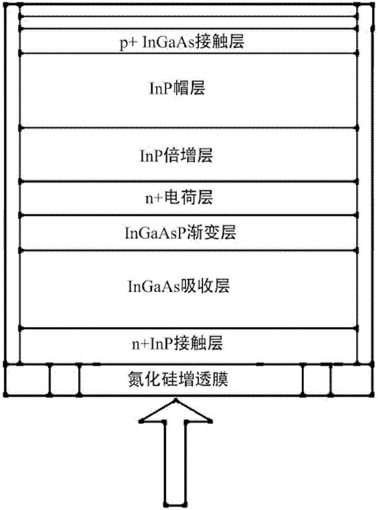
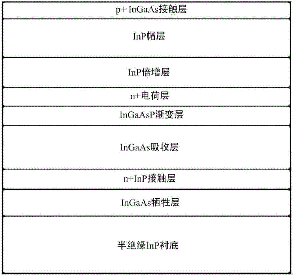
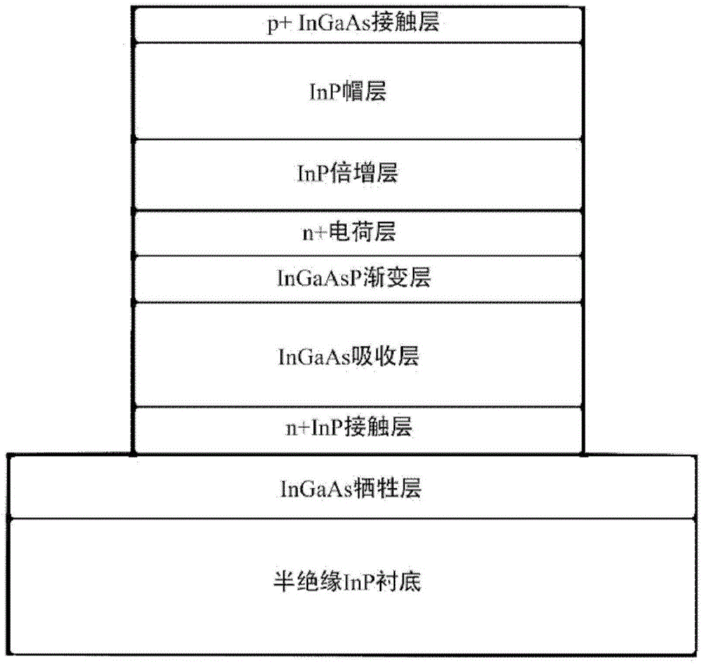
[0029] Step 1: growing an epitaxial wafer, the structure of the epitaxial wafer specifically includes: a semi-insulating InP substrate, In 0.53 Ga 0.47 As sacrificial layer, N-type InP ohmic contact layer, In 0.53 Ga 0.47 As absorption layer, InGaAsP composition graded layer, thickness is 150nm, doping concentration is 1.5×10 17 cm -3 InP charge control layer, InP multiplication layer, InP cap layer, heavily doped P-type In 0.53 Ga 0.47 As ohmic contact layer;

[00...


PUM

PropertyMeasurementUnit
thicknessaaaaaaaaaa
thicknessaaaaaaaaaa
thicknessaaaaaaaaaa

Abstract

The invention discloses a vertical-type avalanche photodiode and a fabrication method thereof. The avalanche photodiode fabrication method comprises steps: a vertical mesa is etched until an In0.53Ga0.47As sacrificial layer; the side wall and the upper surface of the mesa are passivated; the In0.53Ga0.47As sacrificial layer is corroded and removed to realize substrate stripping; an optical antireflection film is prepared on the surface of an N-type InP ohmic contact layer; a P contact metal layer and an N contact metal layer are prepared on the upper surface and the lower surface, and a flat high-reflective mirror metal layer is then formed on the P contact metal layer. Through effective combination between the optical antireflection film and the flat high-reflective mirror metal layer, the response of the avalanche photodiode can be effectively improved. The high-response vertical-type InP / In0.53Ga0.47As avalanche photodiode has the advantages of low cost, simple fabrication process and the like.

Description

technical field [0001] The invention belongs to the field of high-sensitivity infrared detectors, in particular to a preparation method of high-responsivity avalanche photodiodes. Background technique [0002] Avalanche photodiodes have broad application prospects in many weak light detection fields, such as military and civilian applications. Compared with PIN detectors, avalanche photodiodes are semiconductor optoelectronic devices with internal photocurrent gain, which use the impact ionization effect of photogenerated carriers in the depletion layer to obtain avalanche multiplication of photocurrent. With the increase of the speed of the optical communication system, the contradiction between the quantum efficiency and the bandwidth of the device becomes more serious. In order to improve the frequency response of the avalanche photodiode, it is necessary to reduce the epitaxial thickness of the absorber layer. However, reducing the thickness of the absorber layer will r...

Claims


Application Information

Patent Timeline
Patent Type & Authority Applications(China)
IPC IPC(8): H01L31/107H01L31/18
CPCH01L31/1075H01L31/1892
Inventor 陈良惠李慧梅李晓敏李健于海龙宋国峰徐云
Owner INST OF SEMICONDUCTORS - CHINESE ACAD OF SCI
Why Eureka
Try Eureka