Photoetching machine lighting system and method with pupil plane quality monitoring and calibrating functions

A quality monitoring and lighting system technology, applied in the field of semiconductor manufacturing, can solve problems such as the inability to detect the uniformity of the pupil surface of the exposure laser, the inability to detect the shape of the pupil surface of the exposure laser, etc.

Inactive Publication Date: 2015-12-09
SHANGHAI HUALI MICROELECTRONICS CORP
View PDF5 Cites 3 Cited by
  • Summary
  • Abstract
  • Description
  • Claims
  • Application Information

AI Technical Summary

Problems solved by technology

[0008] Although some existing lighting systems using the principle of mirror arrays also have the function of detecting the shape of the pupil surface, they do not detect the shape of the pupil surface through exposure laser irradiation, but use other external light sources, and have no ability to detect the reflected exposure laser light. The shape of the formed pupil surface, of course, cannot detect the uniformity of the pupil surface of the exposure laser

Method used


Image

  • Photoetching machine lighting system and method with pupil plane quality monitoring and calibrating functions
  • Photoetching machine lighting system and method with pupil plane quality monitoring and calibrating functions
  • Photoetching machine lighting system and method with pupil plane quality monitoring and calibrating functions

Examples


Embodiment Construction

[0040] In order to make the content of the present invention clearer and easier to understand, the content of the present invention will be described in detail below in conjunction with specific embodiments and accompanying drawings.

[0041] A more complete understanding of the invention, and its accompanying advantages and features, will be more readily understood by reference to the following detailed description, taken in conjunction with the accompanying drawings, in which:

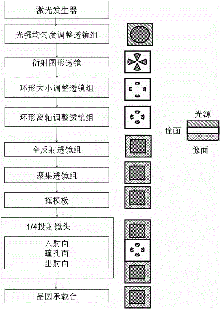
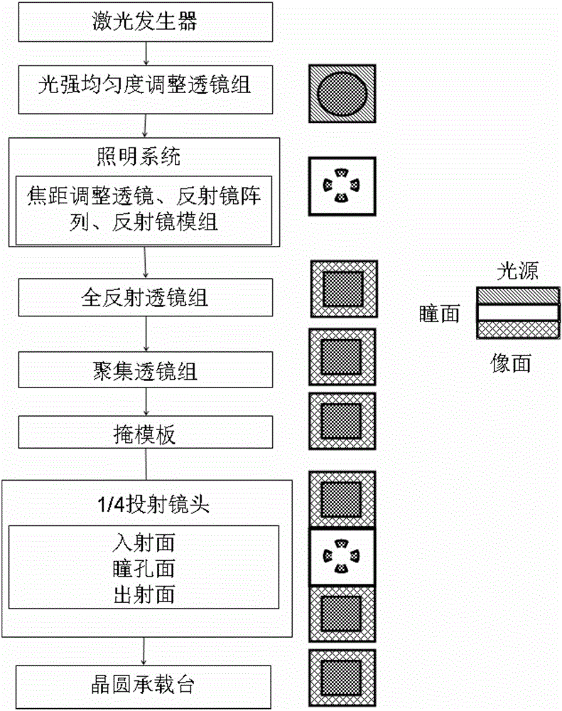
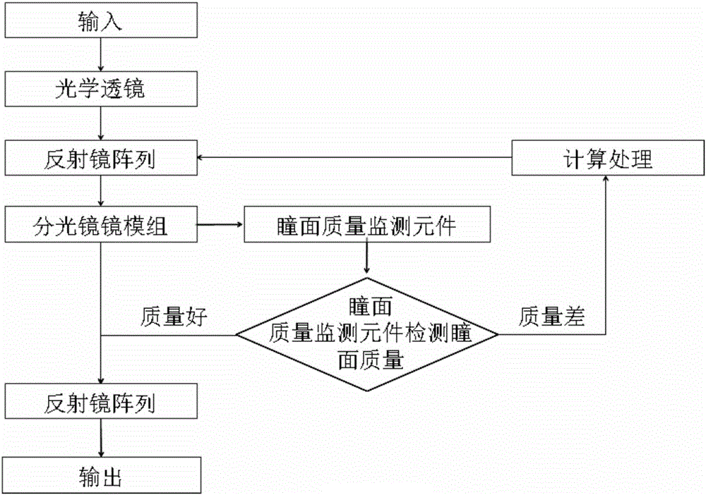
[0042] The technical problem to be solved by the present invention is to provide a lithography machine lighting system with pupil surface quality detection and calibration functions for the above-mentioned defects in the prior art. This lighting system can perform real-time detection, calibration and real-time detection at the first scene where the pupil surface is formed, and control the quality of the pupil surface at the first time, thereby ensuring the final imaging quality of the graphics.

[00...


PUM


Abstract

The invention provides a photoetching machine lighting system and a photoetching machine lighting method with pupil plane quality monitoring and calibrating functions. The method comprises the following steps: emitting laser generated by a laser generator onto a first reflecting mirror so as to reflect the laser to a miniature reflecting mirror array; operating the reflecting mirror array, and adjusting a specific inclination angle of each miniature reflecting mirror unit to enable incident laser to pass through the reflecting mirror array to form a pupil plane shape; projecting a first part of the laser onto a pupil plane quality monitoring element through a light splitting component, acquiring complete pupil plane information through a light intensity value, and judging whether the reflecting mirror array needs to be adjusted; if it is determined that the reflecting mirror array does not need to be adjusted, reflecting a second part of the laser by a second reflecting mirror to enable the laser to enter a subsequent light path for subsequent adjustment; if it is determined that the reflecting mirror array needs to be adjusted, computing pupil plane quality information to obtain a needed adjustment angle of each miniature reflecting mirror unit in the reflecting mirror array, then feeding back to the reflecting mirror array, and performing angle adjustment by the reflecting mirror array according to the needed adjustment angle to calibrate a pupil plane.

Description

technical field [0001] The invention relates to the field of semiconductor manufacturing, and more specifically, the invention relates to a lighting system and method for a lithography machine with functions of pupil surface quality monitoring and calibration. Background technique [0002] Micro-photo-lithography, also known as photolithography, is an important semiconductor manufacturing process. Its function is to use laser irradiation to shrink the circuit graphics on the photomask through a series of multi-group optical elements and then project them on the On the wafer, and then use the photosensitive medium coated on the wafer to retain the circuit pattern, and the wafer can then perform etching or ion implantation process. [0003] In order to obtain the best resolution rate, lithography needs an illumination system to convert the laser light into a state that is most suitable for the imaged circuit pattern for exposure, usually including pupil shape (PupilShape), off...

Claims


Application Information

Patent Timeline
Patent Type & Authority Applications(China)
IPC IPC(8): G03F7/20
Inventor 毛晓明毛智彪
Owner SHANGHAI HUALI MICROELECTRONICS CORP
Why Eureka
Try Eureka