Optimized stack type CIS silicon wafer bonding method

A silicon wafer and bonding technology, which is applied in radiation control devices and other directions, can solve problems such as voids in the silicon wafer bond, achieve the effects of optimizing bonding performance, improving processability, and ensuring stability

Active Publication Date: 2015-12-09
SHANGHAI HUALI MICROELECTRONICS CORP
View PDF3 Cites 9 Cited by
  • Summary
  • Abstract
  • Description
  • Claims
  • Application Information

AI Technical Summary

Problems solved by technology

[0008] The purpose of the present invention is to overcome the above-mentioned defects existing in the prior art, and provide a method for optimizing the bonding

Method used


Image

  • Optimized stack type CIS silicon wafer bonding method
  • Optimized stack type CIS silicon wafer bonding method
  • Optimized stack type CIS silicon wafer bonding method

Examples


Embodiment Construction

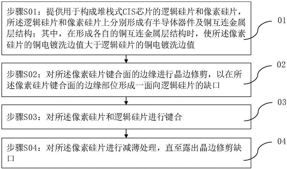
[0027] The specific embodiment of the present invention will be further described in detail below in conjunction with the accompanying drawings.

[0028] It should be noted that, in the following specific embodiments, when describing the embodiments of the present invention in detail, in order to clearly show the structure of the present invention for the convenience of description, the structures in the drawings are not drawn according to the general scale, and are drawn Partial magnification, deformation and simplification are included, therefore, it should be avoided to be interpreted as a limitation of the present invention.

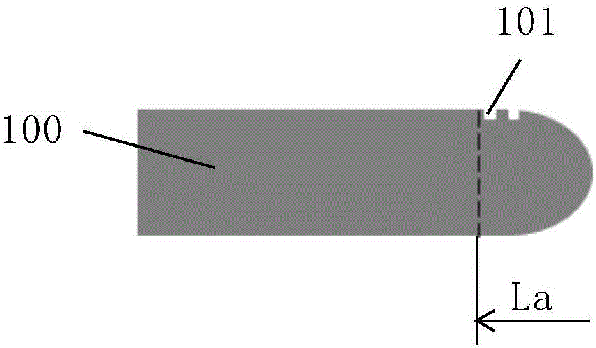
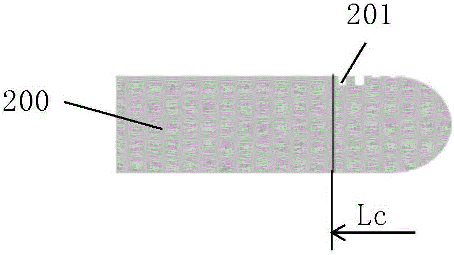
[0029] In the following specific embodiments of the present invention, please refer to figure 1 , figure 1 It is a flowchart of a method for optimizing the bonding of stacked CIS silicon wafers in the present invention; meanwhile, please refer to Figure 2 ~ Figure 6 , Figure 2 ~ Figure 6 is a preferred embodiment of the present invention accordi...


PUM


Abstract

The invention discloses an optimized stack type CIS silicon wafer bonding method. According to the technical scheme of the invention, the bonding of a stack type CIS logic silicon wafer and a pixel silicon wafer is optimized based on the combination adjustment on the copper-electroplating boundary value between the stack type CIS logic silicon wafer and the pixel silicon wafer and the trimming on the crystal boundary of the pixel silicon wafer. In this way, the height difference phenomenon between the boundary region of the logic silicon wafer and a normal region is relieved. Meanwhile, during the bonding process, the pixel silicon wafer is kept away from the region of the logic silicon wafer with a larger height difference, so that no void defect occurs at the crystal boundary interface of the two silicon wafers during the bonding process. Therefore, the bonding performance between the logic silicon wafer and the pixel silicon wafer is optimized. The machinability of the subsequent silicon wafers is improved. Moreover, the stability of the stack type CIS chip manufacturing process is ensured, and the yield is improved.

Description

technical field [0001] The invention relates to the technical field of semiconductor integrated circuit image sensor manufacturing, and more particularly, relates to a method for optimizing the bonding of stacked CIS silicon wafers. Background technique [0002] In the development process of CMOS image sensor (CMOSImageSensor, CIS), if the evolution from front-illuminated (FSI) CIS to back-illuminated (BSI) CIS is a revolution, then the development of back-illuminated CIS to stacked CIS is a great innovation. . At present, CIS is developing towards the direction of high resolution, high pixel and multifunctional integration requirements. [0003] Stacked CIS (Ultra-ThinStacked CMOS Image Sensor) has become the current CIS market due to its flexible manufacturing process brought by the separation of logic and pixel silicon chips, low cost, increased available chip area, and multi-functional chips can be integrated together. High-end products. Stacked CIS is usually formed ...

Claims


Application Information

Patent Timeline
IPC IPC(8): H01L27/146
Inventor 余仁旭张磊姬峰陈昊瑜
Owner SHANGHAI HUALI MICROELECTRONICS CORP
Why Eureka
Try Eureka