Micro-nanofiber structure based wide-spectrum graphene photoconductive detector

A micro-nano optical fiber and detector technology, which is applied to semiconductor devices, circuits, electrical components, etc., can solve the problems of complex detector structure, achieve the effect of simple structure and improve photoelectric detection efficiency

Inactive Publication Date: 2015-12-09
SHANGHAI JIAO TONG UNIV
View PDF3 Cites 8 Cited by
  • Summary
  • Abstract
  • Description
  • Claims
  • Application Information

AI Technical Summary

Problems solved by technology

The structure of ...

Method used


Image

  • Micro-nanofiber structure based wide-spectrum graphene photoconductive detector
  • Micro-nanofiber structure based wide-spectrum graphene photoconductive detector
  • Micro-nanofiber structure based wide-spectrum graphene photoconductive detector

Examples


Embodiment 1

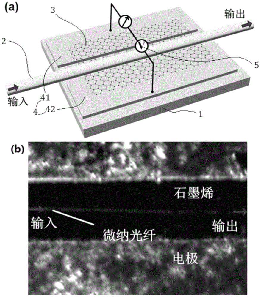
[0019] like figure 1 As shown, the present embodiment includes: substrate 1, micro-nano optical fiber 2, graphene film 3, metal electrode 4 and bias voltage 5, wherein: metal electrode 4 is made on substrate 1, and graphene film 3 is made on metal On the electrode 4 and separate the metal electrode 4 into a first electrode 41 and a second electrode 42, the micro-nano fiber 2 is in contact with the graphene film 3, and the bias voltage 5 is connected to the first electrode 41 and the second electrode 42.

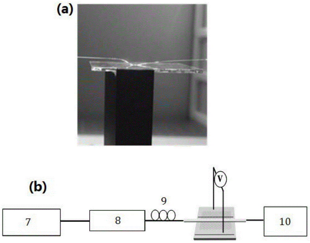
[0020] The micro-nano optical fiber 2 is fixed on the optical fiber holder 6, and the three-dimensional control rotation button on the optical fiber holder 6 is used to adjust the movement in three directions: front and rear, left and right, and up and down.

[0021] like figure 2 As shown in (a), the micro-nano optical fiber 2 is U-shaped and lapped on the graphene film 3, and the two ends are tapered. Precise control of the contact between the nano-fiber 2 and the graphe...


PUM


Abstract

A micro-nanofiber structure based wide-spectrum graphene photoconductive detector in the technical field of optical fiber communication is disclosed. The wide-spectrum graphene photoconductive detector comprises a substrate, micro-nanofiber, a graphene thin film, a metal electrode and bias voltage, wherein the metal electrode is manufactured on the substrate; the graphene thin film is manufactured on the metal electrode and divides the metal electrode into a first electrode and a second electrode; the micro-nanofiber and the graphene thin film are in contact; and the bias voltage is connected with the first electrode and the second electrode. The micro-nanofiber structure based wide-spectrum graphene photoconductive detector has the advantages of wide-spectrum detection, high detection efficiency, low insertion loss and simple structure.

Description

technical field [0001] The invention relates to the technical field of optical fiber communication, in particular to a wide-spectrum graphene photoconductive detector based on a micro-nano optical fiber structure. Background technique [0002] With the maturity of photodetection technology and the gradual expansion of application scope, the requirements for detection rate, effective wavelength and sensitivity of detectors are getting higher and higher, and the rapid development of CMOS technology also requires the gradual development of photodetectors towards integration. Graphene can absorb energy in a broad spectrum range to generate electron-hole pairs, making broadband photodetection possible from infrared to visible to ultraviolet and megahertz bands; and graphene can be perfectly integrated with highly integrated silicon-based devices. It has great advantages in low power consumption and large-scale integration. [0003] After searching the existing technologies, it w...

Claims


Application Information

Patent Timeline
IPC IPC(8): H01L31/0232H01L31/09
CPCH01L31/02327H01L31/09
Inventor 毛俊明周换颖孙晓文潘听邱辞源苏翼凯
Owner SHANGHAI JIAO TONG UNIV
Why Eureka
Try Eureka