Ultraviolet detector

An ultraviolet detector and nano-pillar technology, which is applied in the field of photoelectric sensors, can solve the problems of difficulty, increase the area of ​​semiconductor thin films, and can not obtain thin film resistance at the same time, and achieve the effects of improving sensitivity, improving photoelectric corresponding strength, and increasing sensitivity.

Pending Publication Date: 2015-12-09
宋金会
View PDF3 Cites 9 Cited by
  • Summary
  • Abstract
  • Description
  • Claims
  • Application Information

AI Technical Summary

Problems solved by technology

Therefore, increasing the area of ​​the semiconductor film and reducing the film resistance cannot be obtained at the same time. On the basis of the existing technology, it is very difficult to further improve the sensitivity of the ultraviolet sensor.

Method used


Image

  • Ultraviolet detector
  • Ultraviolet detector
  • Ultraviolet detector

Examples


Embodiment Construction

[0024] In order to make the object, technical solution and advantages of the present invention clearer, the present invention will be described in further detail below in conjunction with specific embodiments and with reference to the accompanying drawings.

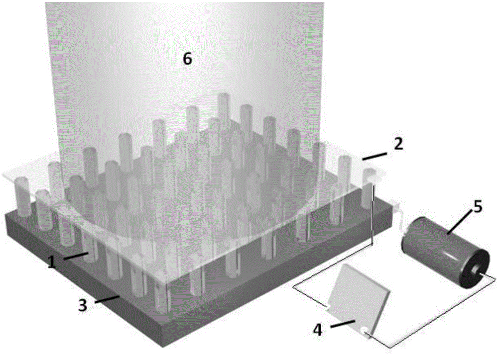
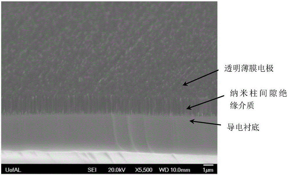
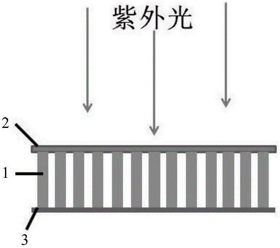
[0025] The ultraviolet detector provided by the present invention comprises three-dimensional semiconductor nanocolumns of the array, flat transparent film electrodes and flat conductive substrates, the top end surface of the semiconductor nanocolumns is connected with one side surface of the transparent film electrodes, and the bottom The end surface is connected to one side surface of the conductive substrate, and the transparent film electrode and the conductive substrate are parallel to each other; a power supply and a current detection unit are connected between the conductive substrate and the transparent film electrode, thereby forming a closed loop , the closed loop is used to measure the resistance change.

[002...


PUM


Abstract

The invention discloses an ultraviolet detector which comprises array-shaped three-dimensional semiconductor nano posts, a tabulate transparent thin-film electrode and a tabulate conductive substrate, wherein the end surfaces at the tops of the semiconductor nano posts are connected with the one side surface of the transparent thin-film electrode, the end surfaces at the bottoms of the semiconductor nano posts are connected with oneside surface of the conductive substrate, the transparent thin-film electrode is parallel to the conductive substrate, a power supply and a current detection unit are connected between the conductive substrate and the transparent thin-film electrode to form a closed loop, and the closed loop is used for measuring the change of a resistance value. The ultraviolet detector has a similar size and the overall thin-film shape as the current ultraviolet detector, a large amount of vertical nano post arrays substitute the overall thin-film structure, the sensitivity of the ultraviolet detector can be improved by increasing the surface area of a semiconductor material on the condition of keeping the two-dimensional area for receiving ultraviolet rays unchanged, the sensitivity limitation of the current ultraviolet detector is successfully broken through, and an ultrahigh-precision nano ultraviolet detector is achieved.

Description

technical field [0001] The invention relates to the technical field of photoelectric sensors, in particular to a high-sensitivity nano-ultraviolet detector. Background technique [0002] Ultraviolet radiation is the strongest radiation in nature. Human eyes cannot see this kind of ultraviolet radiation. Its wavelength range is 180-400nm, which can be divided into UVC radiation (180-280nm), UVB radiation (280-320nm), UVA radiation (320~400nm). Ultraviolet radiation has a strong effect on both organic and inorganic substances. The most important application here is the UVC irradiation of substances for the removal of microbial contamination in beverages, wastewater, food, air and process water. The material properties of plastics and polymers can be modified by exposing organic materials to UV light. UV radiation also enhances the hardness of lenses, adjusts the surface properties of varnishes, and rapidly cures dental fillings. Flames also emit low-level UV radiation, all...

Claims


Application Information

Patent Timeline
Patent Type & Authority Applications(China)
IPC IPC(8): H01L31/09H01L31/036B82Y15/00
CPCH01L31/09H01L31/036
Inventor 宋金会
Owner 宋金会
Why Eureka
Try Eureka