Light emitting diode structure and manufacturing method thereof
A technology for light-emitting diodes and a manufacturing method, which is applied to electrical components, circuits, semiconductor devices, etc., can solve the problems of difficult, incomplete, and easily damaged epitaxial layer peeling off of substrates, and achieves reduction of dislocation defects and epitaxial wafer warping. The effect of reducing the total reflection light absorption and improving the production yield
- Summary
- Abstract
- Description
- Claims
- Application Information
AI Technical Summary
Problems solved by technology
Method used
Image
Examples
Embodiment 1
[0058] This embodiment provides a light emitting diode structure and a manufacturing method, and the specific steps are as follows:
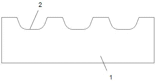
[0059] Such as figure 1 As shown, step (1) firstly provides a sapphire substrate 1, the surface of the substrate 1 has a pattern of grooves 2 and raised structures, and the opening diameter of the groove 2 is 1-5 μm, preferably 4-5 μm. When the opening diameter of the groove is less than 4 μm, the opening of the groove 2 is small, the internal structure of the groove 2 is difficult to manufacture, and the process controllability is poor; when the opening diameter of the groove 2 is greater than 5 μm, it takes longer to grow the first semiconductor Layer 7 is used to cover the groove 2, which greatly increases the manufacturing time of the light emitting diode, but the beneficial effect is not obvious.
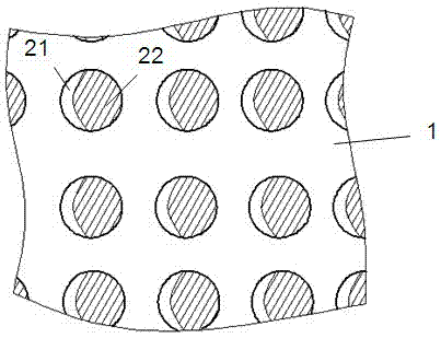
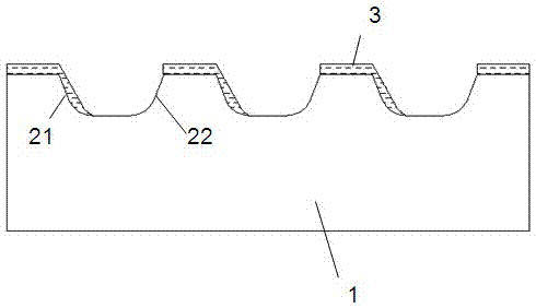
[0060] Such as Figure 2~3 As shown, step (2) grows SiO on the patterned substrate 1 2 The barrier layer 3, defining the sidewall of the groo...
Embodiment 2
[0067] Such as Figure 8~12 As shown, the difference between this embodiment and Embodiment 1 is that the material of the substrate 1 is Si, and after step (3) of Embodiment 1, the AlN transition layer 6 is covered on the region 22 not covered by the sidewall barrier layer, so that Improve the GaN layer 4, Al x Ga 1-x N high temperature resistant layer 5, first semiconductor layer 7, light emitting epitaxial layer 8, second semiconductor layer 9 growth quality.
Embodiment 3
[0069] The difference between this embodiment and Embodiment 2 is that the material of the substrate 1 in this embodiment is SiC, the material of the transition layer 6 is Al, and the transition layer 6 controls the growth polarity of the GaN layer 4 on the substrate 1 to improve the growth of the GaN layer 4. quality.
PUM
| Property | Measurement | Unit |
|---|---|---|
| diameter | aaaaa | aaaaa |
| diameter | aaaaa | aaaaa |
| thickness | aaaaa | aaaaa |
Abstract
Description
Claims
Application Information


