A nano-diamond film with si-v luminescence and its controllable preparation method

A nano-diamond and polycrystalline diamond technology, which is applied in metal material coating process, gaseous chemical plating, coating, etc., can solve the problems that the Si-V luminescence performance of thin films is difficult to control and does not have Si-V luminescence performance.

Active Publication Date: 2017-12-05
ZHEJIANG UNIV OF TECH
View PDF5 Cites 0 Cited by
  • Summary
  • Abstract
  • Description
  • Claims
  • Application Information

AI Technical Summary

Problems solved by technology

The Si-V luminescent center in the nanodiamond film prepared by chemical vapor deposition (CVD) is usually formed by the silicon in the substrate or quartz tube entering the film in the form of non-intentional doping during the film growth process, making the preparation Some of the films have Si-V luminescence, while some films do not have Si-V luminescence properties, that is, the Si-V luminescence properties of the films are difficult to control

Method used


Image

  • A nano-diamond film with si-v luminescence and its controllable preparation method
  • A nano-diamond film with si-v luminescence and its controllable preparation method
  • A nano-diamond film with si-v luminescence and its controllable preparation method

Examples


Embodiment 1

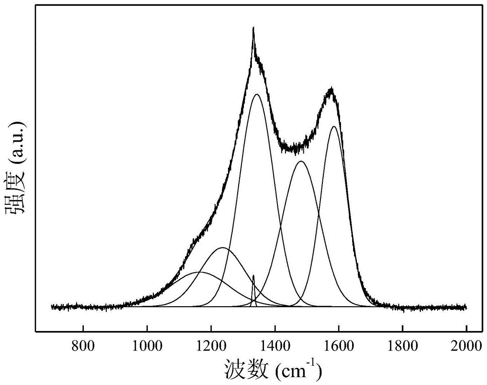
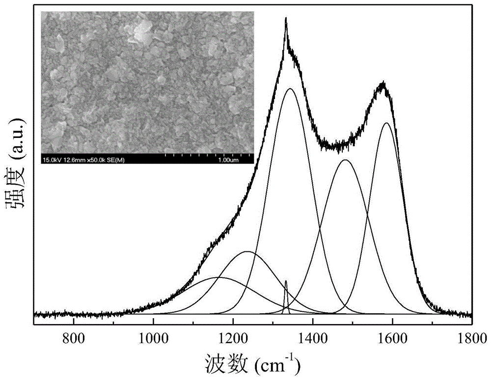
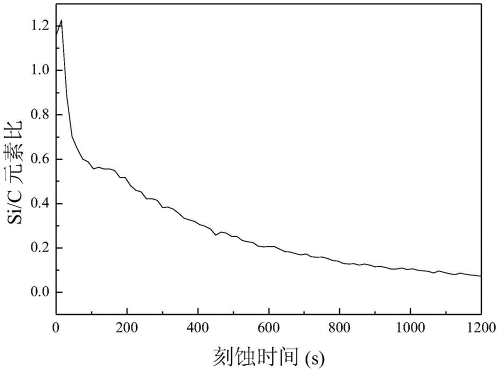
[0023] Polish the polycrystalline diamond substrate with nano-sized diamond powder for about 15 minutes. The polished polycrystalline diamond substrate was ultrasonically oscillated in a diamond micropowder-acetone suspension for 2 hours, then ultrasonically cleaned with deionized water and acetone, and dried, and then used as a substrate for growing a nano-diamond film. Using hot wire chemical vapor deposition (chemical vapor deposition equipment purchased from Shanghai Jiaoyou Diamond Coating Co., Ltd., model JUHF CVD001), using acetone as the carbon source, acetone was brought into the reaction chamber by hydrogen bubbling, and the reaction chamber The temperature is controlled at 600-700° C., the preparation time is 4 hours, and a nano-diamond film with a thickness of 4-6 μm is prepared. Using a 100keV isotope separator, the injection energy is 80keV, and the nano-diamond film is subjected to 10 14 cm -2 silicon ion implantation treatment to obtain silicon ion implanted ...


PUM

PropertyMeasurementUnit
thicknessaaaaaaaaaa

Abstract

The invention discloses a method for preparing a nano-diamond film with Si-V luminescence: on a polycrystalline diamond substrate, a nano-diamond film is prepared by a hot wire chemical vapor deposition method; silicon ion implantation is performed on the nano-diamond film, and the implanted The dose is 1013-1015cm-2 to obtain a silicon ion-implanted film; the silicon-ion-implanted film is annealed at a temperature of 800-900°C and a pressure of 3000-5000Pa for 30-60 minutes to obtain an annealed film; The nano-diamond film with Si-V luminescence is obtained by keeping the temperature in air at 600° C. for 30-60 minutes. In the present invention, quantitative silicon is incorporated into the nano-diamond film by ion implantation, so that the doping dose of silicon is quantified, and the controllable preparation of the nano-diamond film with Si-V luminescent properties is realized, and the prepared nano-diamond The thin film has Si‑V light emitting properties.

Description

(1) Technical field [0001] The invention relates to a nano-diamond thin film with Si-V luminescence (the luminescence peak in the photoluminescence spectrum is at 738nm) and a controllable preparation method thereof. (2) Background technology [0002] There are more than 500 luminescent centers in diamond, among which there are three most typical luminescent centers: nitrogen-vacancy (N-V), NE8 and silicon-vacancy (Si-V) centers, which have been confirmed as bright and stable room temperature single photon sources , has very important scientific significance and engineering value in the application of single photon sources, quantum information processing, optoelectronic devices, biomarkers, semiconductor devices and field emission displays. [0003] The luminescence peak of the Si-V luminescence center in diamond is located at 738nm in the photoluminescence spectrum (PL spectrum), the line width is narrow (~5nm), and the luminescence lifetime is very short (1.2ns), making Si...

Claims


Application Information

Patent Timeline
Patent Type & Authority Patents(China)
IPC IPC(8): C23C16/27C23C16/56
Inventor 胡晓君徐辉
Owner ZHEJIANG UNIV OF TECH
Why Eureka
Try Eureka