Film transistor array substrate, preparation method thereof and liquid crystal panel

A thin-film transistor and array substrate technology, applied in the field of liquid crystal display, can solve the problems of leakage current channel, breakdown, large aperture ratio, etc., and achieve the effect of improving driving capability, increasing on-state current, and increasing aspect ratio

Inactive Publication Date: 2015-12-16
SHENZHEN CHINA STAR OPTOELECTRONICS TECH CO LTD
View PDF3 Cites 12 Cited by
  • Summary
  • Abstract
  • Description
  • Claims
  • Application Information

AI Technical Summary

Problems solved by technology

In order to ensure the resolution of the display screen, the area of ​​the pixel area needs to be as small as possible, and the aperture ratio needs to be as large as possible. Therefore, the driving thin film transistor and peripheral circuits cannot exceed a certain area, which determines the channel area width of the thin film transistor. W cannot be made too wide. In this case, it is necessary to increase the width-to-length ratio of the channel region of the thin film transistor, which can only be solved by reducing the length L. However, reducing the length L of the channel region of the thin film transistor to a certain extent will cause leakage. Phenomena such as current and channel breakdown, causing thin film transistors to fail to work

Method used


Image

  • Film transistor array substrate, preparation method thereof and liquid crystal panel
  • Film transistor array substrate, preparation method thereof and liquid crystal panel
  • Film transistor array substrate, preparation method thereof and liquid crystal panel

Examples


Embodiment Construction

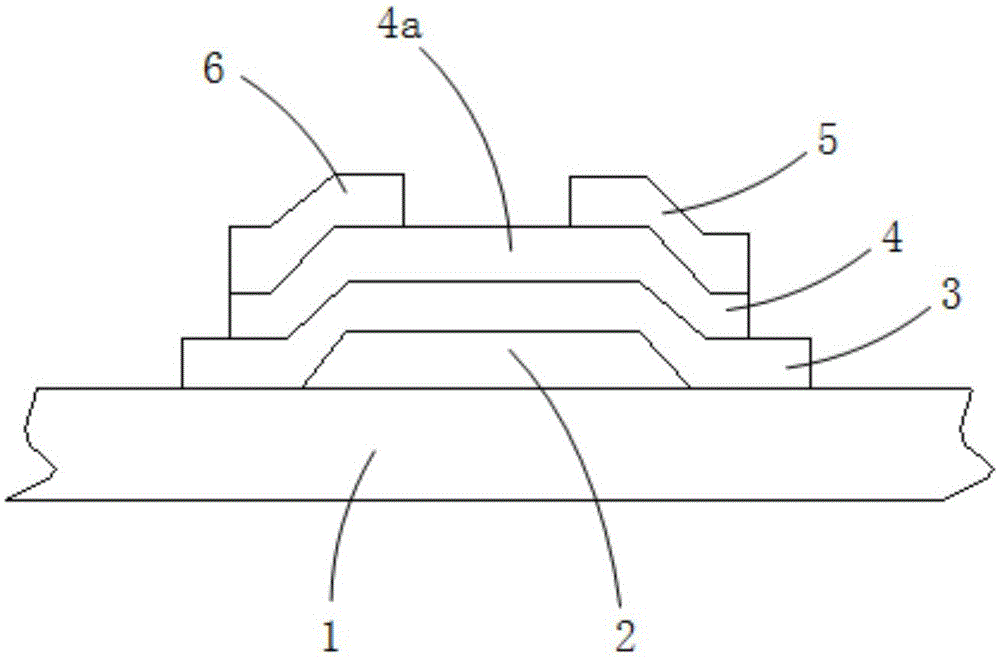
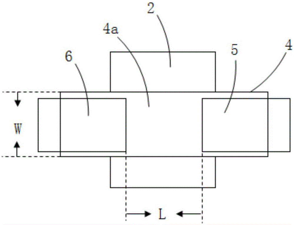
[0031] In order to make the objectives, technical solutions, and advantages of the present invention clearer, the specific embodiments of the present invention will be described in detail below with reference to the accompanying drawings. Examples of these preferred embodiments are illustrated in the drawings. The embodiments of the present invention shown in the drawings and described in accordance with the drawings are merely exemplary, and the present invention is not limited to these embodiments.

[0032] Here, it should also be noted that, in order to avoid obscuring the present invention due to unnecessary details, only the structure and / or processing steps closely related to the solution according to the present invention are shown in the drawings, and the Other details not relevant to the present invention.

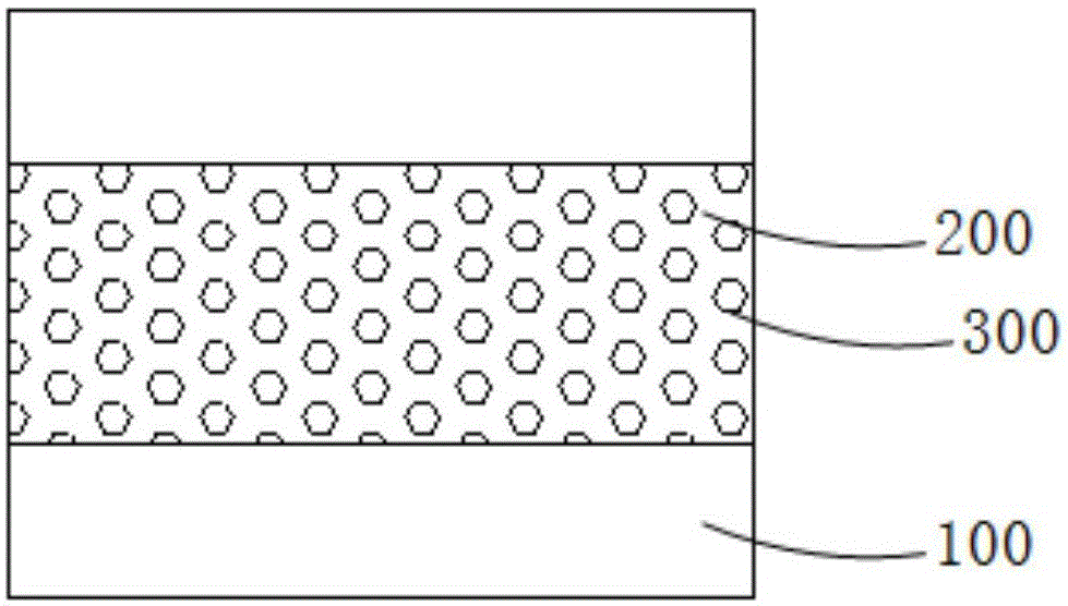
[0033] Such as image 3 As shown, the liquid crystal panel provided in this embodiment includes a thin film crystal array substrate 100 and a filter substrate 200 tha...


PUM


Abstract

The invention discloses a film transistor array substrate which comprises a plurality of film transistors arranged on one glass substrate in an array manner. Each film transistor comprises a grid electrode formed on the glass substrate, a grid electrode insulating layer covering the grid electrode, an active layer arranged on the grid electrode insulating layer, and a source electrode and a drain electrode which are formed on the active layer, wherein the source electrode and the drain electrode are spaced in a first direction, and the region, corresponding to the interval between the source electrode and the drain electrode, of the active layer is a channel region; the surface, facing the active layer and at least corresponding to the channel region, of the grid electrode insulating layer is provided with a plurality of protruding structures, and a wrinkled surface with a plurality of grooves is formed; and the surface, facing the grid electrode insulating layer, of the active layer is totally engaged with the surface of the grid electrode insulating layer. The invention further discloses a preparation method of the film transistor array substrate and a liquid crystal panel comprising the film transistor array substrate.

Description

Technical field [0001] The present invention relates to the technical field of liquid crystal display, in particular to a thin film transistor array substrate and a preparation method thereof, and also to a liquid crystal panel containing the thin film transistor array substrate. Background technique [0002] Liquid crystal display (LiquidCrystalDisplay, LCD), is a flat ultra-thin display device, it is composed of a certain number of color or black and white pixels, placed in front of the light source or reflector. Liquid crystal displays have very low power consumption, high image quality, small size, and light weight, so they are very popular and become the mainstream of displays. At present, the liquid crystal display is mainly a thin film transistor (TFT) liquid crystal display, and the liquid crystal panel is the main component of the liquid crystal display. [0003] A commonly used liquid crystal panel at least includes a thin film transistor array substrate and a color filt...

Claims


Application Information

Patent Timeline
Patent Type & Authority Applications(China)
IPC IPC(8): H01L29/786H01L21/336H01L27/12G02F1/1362G02F1/1368
CPCG02F1/1368H01L21/28008H01L21/28158H01L29/42384H01L29/78609H01L29/78696H01L2029/42388G02F1/1362H01L27/1222H01L29/66742
Inventor 武岳李珊雍玮娜
Owner SHENZHEN CHINA STAR OPTOELECTRONICS TECH CO LTD
Why Eureka
Try Eureka