Injection molding based CSP packaging structure and manufacturing process

A technology of packaging structure and injection molded parts, which is applied in the direction of electrical components, semiconductor devices, circuits, etc., can solve problems such as the difficulty in ensuring the quality of chip-level packaging LEDs, the difficulty in controlling the shape and amount of fluorescent glue, and the difficulty in controlling the uniformity of the thickness of fluorescent glue. , to achieve the effect of improving light extraction efficiency and good reflection performance

Active Publication Date: 2015-12-16
HONGLI ZHIHUI GRP CO LTD
View PDF8 Cites 14 Cited by
  • Summary
  • Abstract
  • Description
  • Claims
  • Application Information

AI Technical Summary

Problems solved by technology

Although this process is simple, it is difficult to control the shape and dosage of the fluorescent glue and the thickness uniformity of the fluorescent glue everywhere because the fluorescent glue has a certain fluidity when packaging the fluorescent glue. Difficult to guarantee quality

Method used


Image

  • Injection molding based CSP packaging structure and manufacturing process
  • Injection molding based CSP packaging structure and manufacturing process
  • Injection molding based CSP packaging structure and manufacturing process

Examples


Embodiment 1

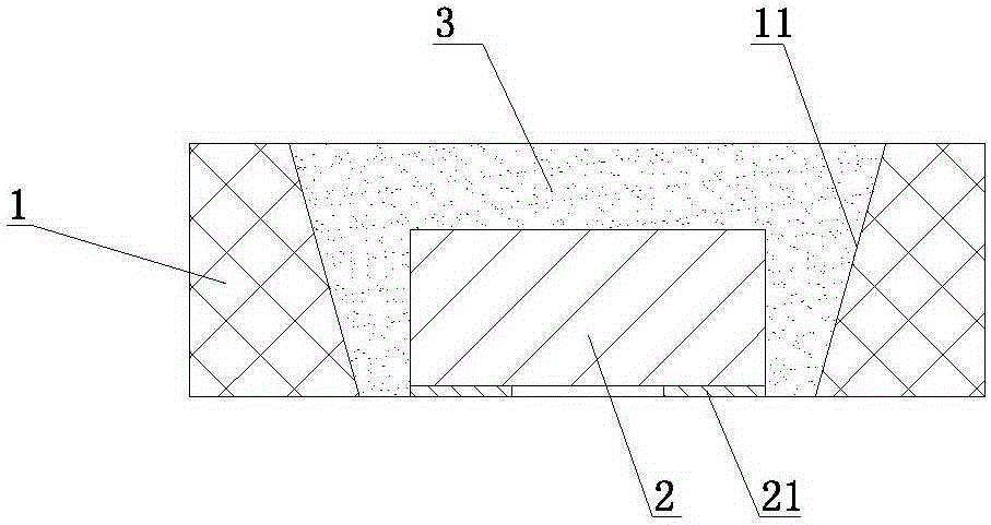
[0046] Such as figure 1 As shown, a CSP packaging structure based on injection molded parts includes an injection molded part body 1 through injection molding. One-sided light emission, the injection molded part body 1 is provided with a through hole 11, the through hole 11 is in the shape of a truncated cone with a large top and a small bottom, so that the through hole 11 can make it easier for the fluorescent glue 3 to flow downward so that the fluorescent glue can be filled to the full. The purpose of the hole; in addition, the through hole 11 of this structure helps to reflect the light of the LED chip 2, thereby achieving the purpose of improving light efficiency; a layer of reflective layer is coated on the inner wall of the through hole 11, so that the reflection of light Better performance, improve light efficiency. The through hole 11 is provided with an LED chip 2, and the LED chip 2 is provided with an electrode 21. The lower surface of the electrode 21 is flush wi...

Embodiment 2

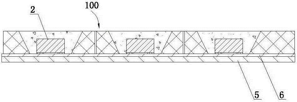
[0049] Such as figure 2 As shown, a CSP packaging structure based on injection molded parts includes an injection molded part body 1 through injection molding. One-sided light emission, the injection molded part body 1 is provided with a through hole 11, the through hole 11 is in the shape of a truncated cone with a large top and a small bottom, so that the through hole 11 can make it easier for the fluorescent glue 3 to flow downward so that the fluorescent glue can be filled to the full. The purpose of the hole; in addition, the through hole 11 of this structure helps to reflect the light of the LED chip 2, thereby achieving the purpose of improving light efficiency; a layer of reflective layer is coated on the inner wall of the through hole 11, so that the reflection of light Better performance, improve light efficiency. The through hole 11 is provided with an LED chip 2, and the LED chip 2 is provided with an electrode 21. The lower surface of the electrode 21 protrudes ...

Embodiment 3

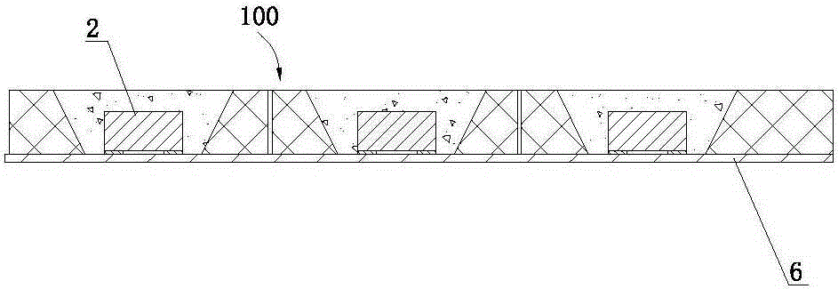
[0053] Such as image 3 As shown, the LED device based on injection molding includes a CSP packaging structure based on injection molding and a substrate 4 .

[0054] Such as figure 1 As shown, the CSP packaging structure based on injection molded parts includes the injection molded part body 1 through injection molding. To emit light, the main body 1 of the injection molded part is provided with a through hole 11. The through hole 11 is a truncated cone with a large upper part and a smaller lower part. In this way, the through hole 11 allows the fluorescent glue 3 to flow downward more easily so that the fluorescent glue can fill the through hole. Purpose; In addition, the through hole 11 of this structure helps to reflect the light of the LED chip 2, thereby achieving the purpose of improving light efficiency; a layer of reflective layer is coated on the inner wall of the through hole 11, so that the reflection performance of light is better Well, improve the light extract...


PUM


Abstract

The invention discloses an injection molding based CSP packaging structure and a manufacturing process. The packaging structure comprises an injection molding body formed through injection molding, the injection molding body is provided with through holes, the through holes are internally provided with LED chips, the LED chips are provided with electrodes, and the lower surfaces of the electrodes are in flush with the lower surface of the injection molding body or project out of the lower surface of the injection molding body; and the through holes are filled up with fluorescent glue covering the side surfaces and the top surfaces of the LED chips. The manufacturing method is as follows: injection-molding an injection molding, arranging a fixation membrane on a support plate, arranging the injection molding on the fixation membrane, fixing the LED chips, filling the through holes with the fluorescent glue, cutting, and separating the support plate from an isolation membrane. According to the invention, the technical problems of difficult control of the shape and the application amount of the fluorescent glue, difficult control of thickness uniformity of the fluorescent glue at each position, and difficulty in ensuring the quality of a chip scale package LED are solved.

Description

technical field [0001] The invention relates to a CSP packaging structure and manufacturing process based on injection molded parts. Background technique [0002] A new type of chip-scale package LED (CSPLED; ChipScale LED) based on flip-chip [0003] Package LED) has electrodes on the bottom of the chip, and directly encapsulates the colloid on the upper surface and side of the chip, so that the electrodes on the bottom are exposed. Since this packaging structure has no support, it can reduce the packaging cost, reduce the volume, and improve the electric current. contact performance. [0004] The existing chip-level packaged LEDs usually emit light from five sides, that is, the top surface and four sides of the LED can emit light. The packaging process of this kind of LED is relatively simple. The specific process is: first lay a fixed film on the carrier plate , and then fix the LED chip on the fixing film, and then encapsulate the fluorescent glue on the LED chip. The...

Claims


Application Information

Patent Timeline
Patent Type & Authority Applications(China)
IPC IPC(8): H01L33/48H01L33/54H01L33/60H01L33/64H01L33/00
CPCH01L33/48H01L33/54H01L33/60H01L33/64H01L2933/0033H01L2933/005H01L2933/0058H01L2933/0075
Inventor 熊毅杜金晟朱富斌李坤锥
Owner HONGLI ZHIHUI GRP CO LTD
Why Eureka
Try Eureka