Making method of nuclear track etching membrane
A technology of nuclear track etching and manufacturing method, applied in chemical instruments and methods, membrane technology, semi-permeable membrane separation, etc., can solve problems such as being unsuitable for mass production, difficult to single-cone micropore diameter D1, difficult to operate, etc. , to achieve the effect of easy implementation, low cost and simple process
- Summary
- Abstract
- Description
- Claims
- Application Information
AI Technical Summary
Problems solved by technology
Method used
Image
Examples
Embodiment 1
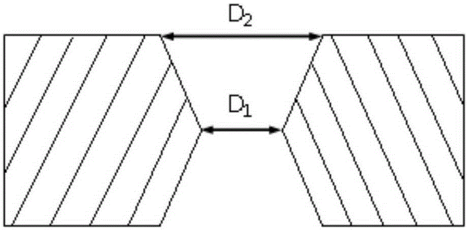
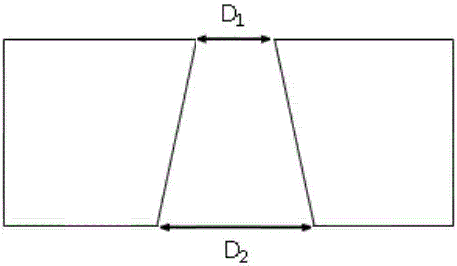
[0028] This embodiment is used to illustrate the manufacturing method of the nuclear track etching film provided by the present invention. Specific steps are as follows:
[0029] Irradiation: A polypropylene film with a thickness of 35 μm is selected as the base film, and a sulfide ion beam with an energy of 120-500 MeV is generated on the tandem accelerator of the China Institute of Atomic Energy, and the beam intensity is 0.1nA-1mA, which is radiated on the base film , the irradiation time is 0.1-0.8 seconds, so that the latent tracks generated by the irradiation penetrate the polymer base film, and the latent track density formed on the base film after irradiation is 1×10 5 / cm 2 ;
[0030] Coating anti-etching coating: coating anti-etching ink (Taiwan Chuan Yu, model: PR3000) on one side of base film after irradiation, the thickness of the anti-etching ink coating that makes is 5 μm;
[0031] Etching: put the base film coated with an anti-etching coating in H2 with a co...
Embodiment 2
[0037] This embodiment is used to illustrate the manufacturing method of the nuclear track etching film provided by the present invention. Specific steps are as follows:
[0038] Irradiation: Use a polyethylene terephthalate (PET) film with a thickness of 25 μm as the base film, and generate a sulfur ion beam with an energy of 120-500 MeV on the tandem accelerator of the China Institute of Atomic Energy. 0.1nA ~ 1mA, radiate on the base film, the irradiation time is 0.1 ~ 0.8 seconds, so that the latent track generated by the irradiation runs through the polymer base film, and the latent track density formed on the base film after irradiation is 1× 10 5 / cm 2 ;
[0039] Apply anti-etching coating: one side of base film after irradiation is coated with anti-etching glue (Rentong, model: S-338), the thickness of the anti-etching glue coating that makes is 3 μ m;
[0040] Etching: put the base film coated with an anti-etching coating in a NaOH solution with a concentration of...
PUM
| Property | Measurement | Unit |
|---|---|---|
| Thickness | aaaaa | aaaaa |
| Thickness | aaaaa | aaaaa |
| Concentration | aaaaa | aaaaa |
Abstract
Description
Claims
Application Information


