Light source assembly used for backlight module, backlight module and liquid crystal displayer
A technology for backlight modules and light source components, applied in instruments, optics, nonlinear optics, etc., can solve the problems of increasing color resist film thickness, aggravating dark-state light leakage, increasing costs, etc., and achieves the improvement of color gamut and color purity. Effect
- Summary
- Abstract
- Description
- Claims
- Application Information
AI Technical Summary
Problems solved by technology
Method used
Image

Examples
Embodiment 1
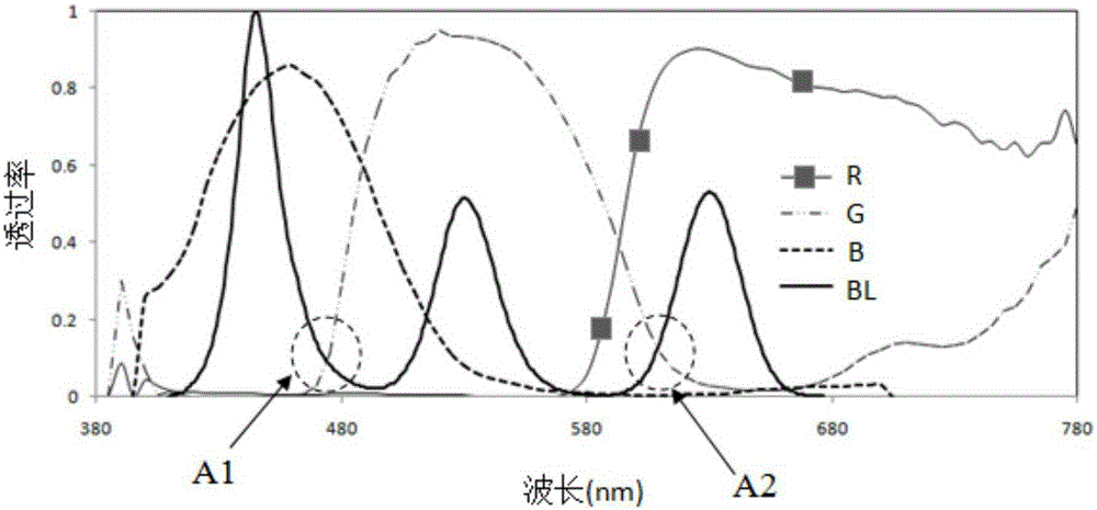
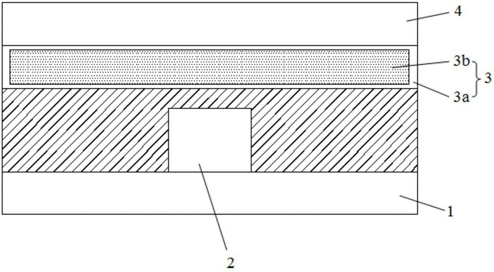
[0029] This embodiment provides a light source assembly for a backlight module, such as figure 2 As shown, the light source assembly includes a substrate 1 and an LED chip 2 packaged on the substrate 1, the LED chip 2 is provided with an optical conversion part 3, and the optical conversion part 3 is used to convert the light emitted by the LED chip 2 Monochromatic light is converted to white light. Specifically, the LED chip 2 may be a blue LED chip or an ultraviolet LED chip. The optical conversion part 3 includes a glass box body 3a and fluorescent powder or phosphor powder 3b packaged in the glass box body 3a.
[0030] Wherein, the fluorescent powder or phosphorescent powder 3b can be fluorescent powder or phosphorescent powder of quantum dot material, such as CdS, ZnS, PbS, CdSe, ZnSe, PbSe, CdTe, CdTeSe, InP, AgInS, CuInS, CuInSe one or several. The phosphor or phosphor powder can also be traditional phosphor powder or phosphor powder, such as nitride, oxynitride, si...
Embodiment 2
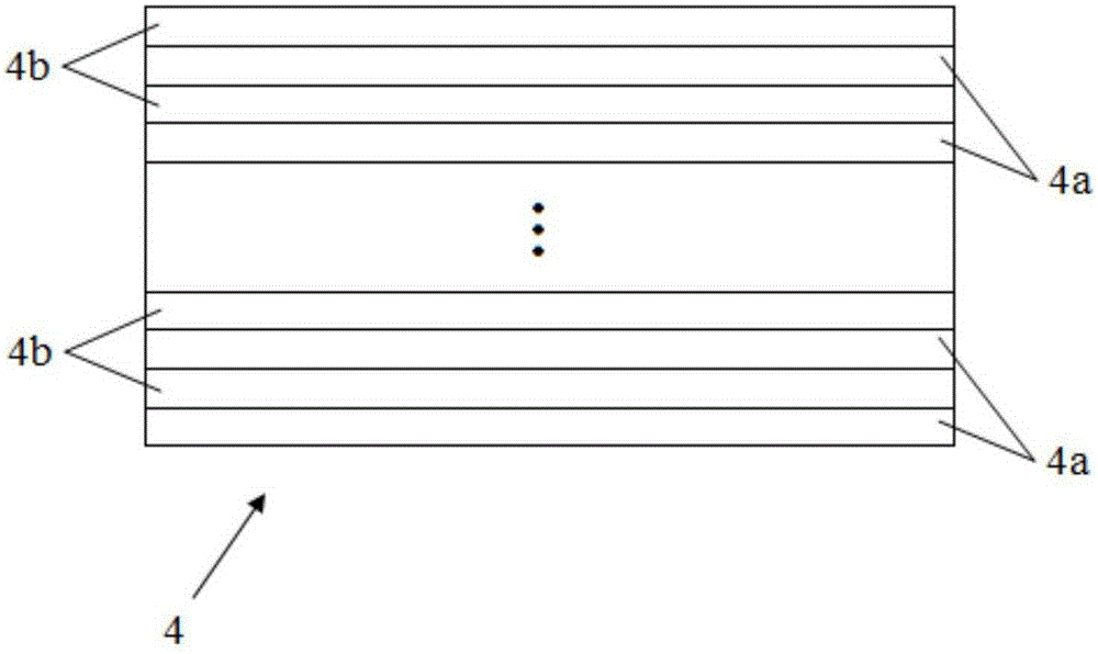
[0042] This embodiment provides a side-type backlight module, such as Figure 5 As shown, the backlight module includes a backplane 10 and a reflective sheet 20, a light guide plate 30, and an optical film set 40 sequentially arranged on the backplane 10. The backlight module also includes a light source assembly 50, and the light source assembly 50 is arranged on the guide Between the side of the light board 30 and the side wall of the backplane 10 . Wherein, the light source assembly 50 adopts the light source assembly provided in the first embodiment. refer to Figure 5 and combine figure 2 The light emitted by the LED chip 2 sequentially passes through the optical conversion part 3 and the filter film set 4 and then enters the light guide plate 30 , and then is emitted from the optical film set 40 above the light guide plate 30 to be provided to the liquid crystal panel.
[0043] This embodiment also provides a direct type backlight module, such as Figure 6 As shown,...
PUM
| Property | Measurement | Unit |
|---|---|---|
| Thickness | aaaaa | aaaaa |
Abstract
Description
Claims
Application Information