Magnetron sputtering method for depositing thin film

A magnetron sputtering and thin-film technology, applied in the field of magnetron sputtering, can solve problems such as pressure rise, inability to fill through-silicon holes, process failure, etc., and achieve the effects of improving quality, reducing deposition rate and deposition density

Active Publication Date: 2015-12-30
BEIJING NAURA MICROELECTRONICS EQUIP CO LTD
View PDF8 Cites 8 Cited by
  • Summary
  • Abstract
  • Description
  • Claims
  • Application Information

AI Technical Summary

Problems solved by technology

[0006] In the traditional technology, the process of depositing thin films in TSVs using magnetron sputtering equipment is as follows: the process gas is introduced into the reaction chamber 1; DC bias is applied to the target 2 for initiation; 2, and apply RF bias on the lower electrode 6 to deposit the film. In this step, the moment the DC bias applied to the target 2 increases, the process near the target 2 A large amount of gas is ionized, resulting in an instantaneous increase in the pressure in chamber 1
When the pressure in the reaction chamber 1 rises instantaneously, a large amount of ionized process gas will enter the lower part of the reaction chamber 1 through the gap between the plurality of claws 51 on the metal snap ring 5; The RF bias is easy to couple in the lower part of the reaction chamber 1, causing the lower part of the reaction chamber 1 to glow; after the lower part of the reaction chamber 1 glows, the energy of the RF bias is used to maintain the gas glow, and it cannot be placed on the mechanical chuck 4 An effective negative bias is formed to attract the metal plasma, resulting in the inability of the metal ions to effectively fill the TSVs, resulting in process failure

Method used


Image

  • Magnetron sputtering method for depositing thin film
  • Magnetron sputtering method for depositing thin film
  • Magnetron sputtering method for depositing thin film

Examples


Embodiment 1

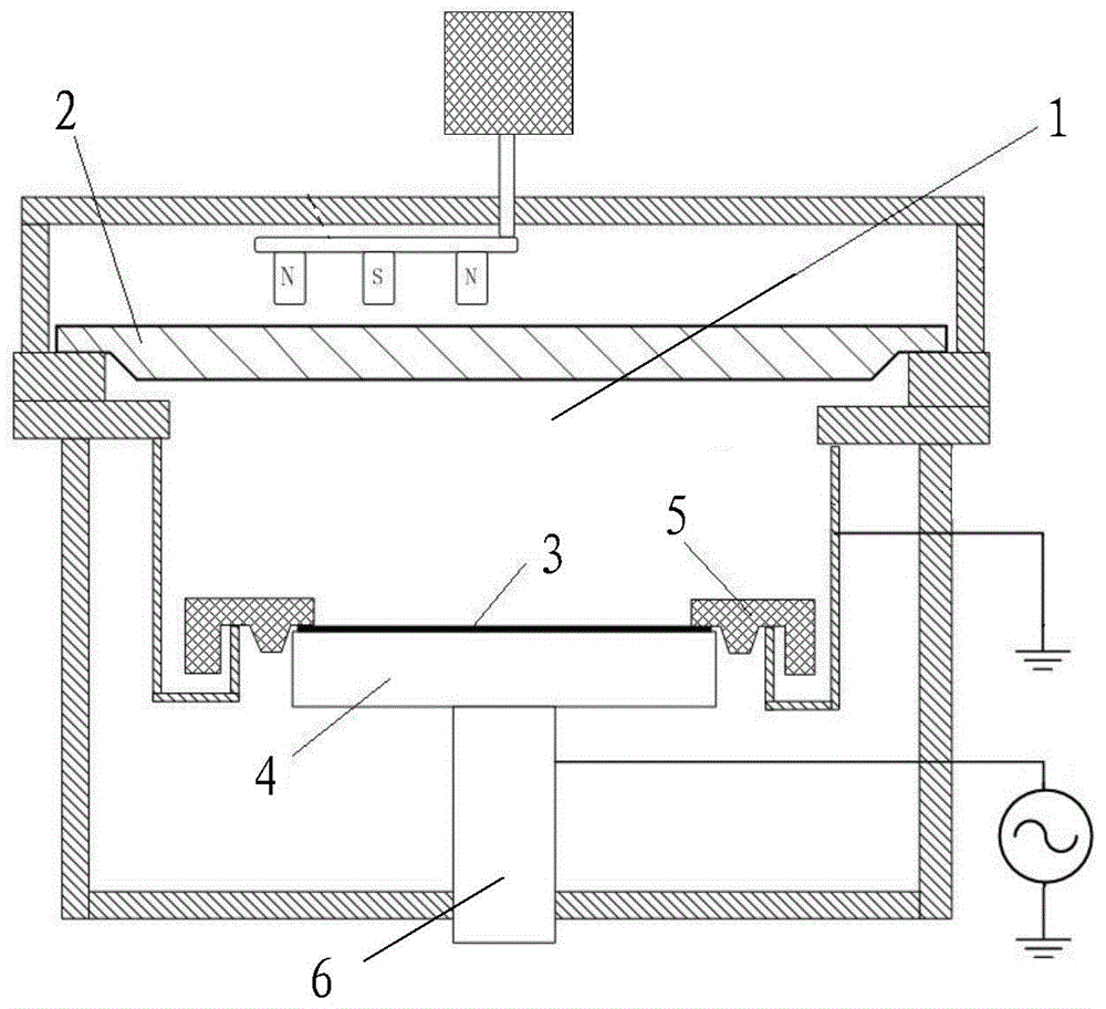
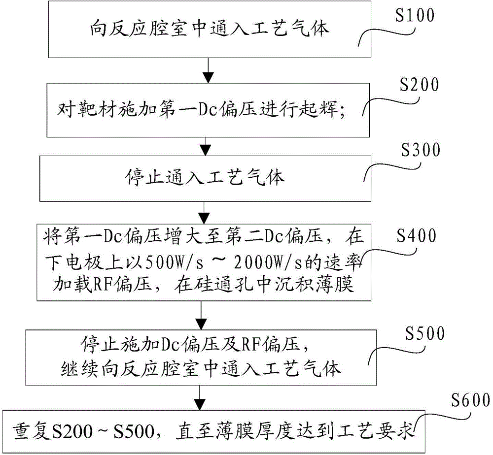
[0052] In this embodiment, a Ti film is deposited in the TSV as a barrier layer. In this embodiment, magnetron sputtering equipment is used to deposit the Ti film. In combination with Table 1, the specific deposition steps of this embodiment are described as follows:

[0053] (1) feed argon gas: feed argon gas 7s in the reaction chamber of magnetron sputtering equipment; Control the flow rate of argon gas to be 100 sccm;

[0054] (2) Starting: Turn on the DC power supply, apply a DC bias to the target, and control the power of the DC bias to 1000W; control the starting time to 2s;

[0055] It should be noted that, in this step, the argon gas was continuously fed and the flow rate of 100 sccm was maintained.

[0056] (3) Depressurization: stop the feeding of argon for 2s, reduce the pressure in the reaction chamber;

[0057] (4) Thin film deposition: increase the DC bias voltage of 1000W applied to the target to 38000W, and apply a 600W RF bias voltage on the lower electrode a...


PUM


Abstract

The invention discloses a magnetron sputtering method for depositing a thin film. The method comprises the following steps that within first preset time, process gas is introduced into a reaction chamber; within second preset time, first DC bias is exerted on a target material, and lighting-up is carried out; within third preset time, introducing of the process gas is stopped; within fourth preset time, the first DC bias is increased to be second DC bias, RF bias is loaded on a lower electrode at the speed of 500 W/s-2000 W/s, and the thin film is deposited into a silicon through hole; within fifth preset time, exerting of the DC bias and the RF bias is stopped, and the process gas continues to be introduced into the reaction chamber; the steps are repeated until the thickness of the thin film meets the process requirement. The magnetron sputtering method for depositing the thin film can effectively prevent the lower portion of the reaction chamber from being lightened and ensure that the thin film can deposit in the silicon through hole smoothly.

Description

technical field [0001] The invention relates to the field of semiconductor manufacturing, in particular to a magnetron sputtering method for depositing thin films. Background technique [0002] Magnetron sputtering is a type of physical vapor deposition, which is widely used in the deposition of metal layers in the manufacturing process of integrated circuits. Through Silicon Via (TSV) technology is a new technical solution for interconnection of stacked chips in three-dimensional integrated circuits. This technology can greatly reduce the interconnection delay between chips and produce chips with more complex structures and stronger performance. , has become the most eye-catching technology in the current electronic packaging technology. [0003] The application of magnetron sputtering in TSV technology is mainly to deposit barrier layer and copper seed layer inside TSV. Among them, the function of the barrier layer is to prevent copper from diffusing into silicon or sili...

Claims


Application Information

Patent Timeline
Patent Type & Authority Applications(China)
IPC IPC(8): C23C14/35
Inventor 杨敬山
Owner BEIJING NAURA MICROELECTRONICS EQUIP CO LTD
Why Eureka
Try Eureka