Flexible active pressure/strain sensor structure and manufacturing method thereof

A technology of strain sensor and manufacturing method, which is applied in semiconductor/solid-state device manufacturing, electric/magnetic solid deformation measurement, measurement of property and force applied to piezoelectric devices, etc., can solve problems such as complex structure and process, and achieve structure and process Simple, simple signal processing at the output end, and the effect of reducing process steps and costs

Active Publication Date: 2015-12-30
SHANGHAI INTEGRATED CIRCUIT RES & DEV CENT
View PDF6 Cites 23 Cited by
  • Summary
  • Abstract
  • Description
  • Claims
  • Application Information

AI Technical Summary

Problems solved by technology

The Chinese invention patent application with the publication number CN104613861A discloses a flexible active strain or pressure sensor structure and preparation method. The method of electric thin film, its structure and process are more complicated

Method used


Image

  • Flexible active pressure/strain sensor structure and manufacturing method thereof
  • Flexible active pressure/strain sensor structure and manufacturing method thereof
  • Flexible active pressure/strain sensor structure and manufacturing method thereof

Examples


Embodiment Construction

[0032] The specific embodiment of the present invention will be further described in detail below in conjunction with the accompanying drawings.

[0033] It should be noted that, in the following specific embodiments, when describing the embodiments of the present invention in detail, in order to clearly show the structure of the present invention for the convenience of description, the structures in the drawings are not drawn according to the general scale, and are drawn Partial magnification, deformation and simplification are included, therefore, it should be avoided to be interpreted as a limitation of the present invention.

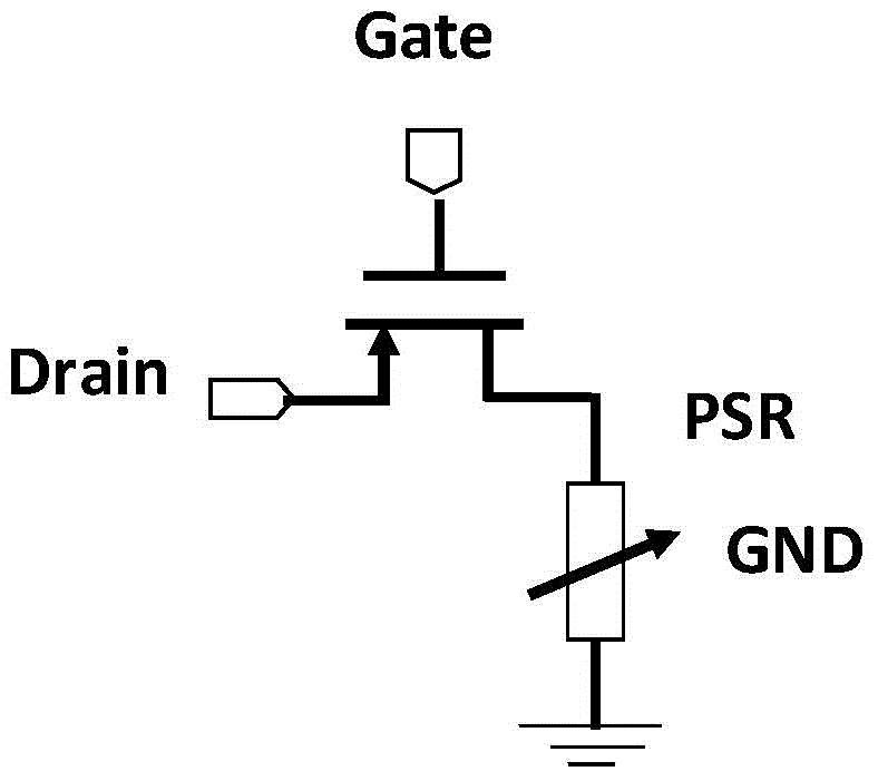
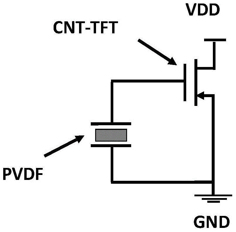
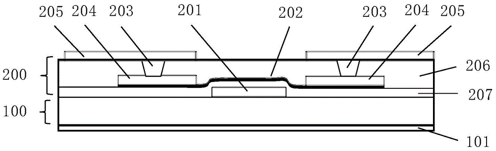
[0034] In the following specific embodiments of the present invention, please refer to figure 2 , figure 2 It is a structural schematic diagram of a flexible active pressure / strain sensor structure in a preferred embodiment of the present invention. Such as figure 2 As shown, a flexible active pressure / strain sensor structure of the present inv...


PUM

PropertyMeasurementUnit
thicknessaaaaaaaaaa
thicknessaaaaaaaaaa

Abstract

The invention discloses a flexible active pressure/strain sensor structure and a manufacturing method thereof. A carbon nano thin film transistor device array is directly integrated on a flexible piezoelectric thin film, the threshold voltage of carbon nano thin film transistor devices can be directly changed by change of the electric charge of the piezoelectric thin film, the strain and pressure magnitude of the piezoelectric thin film can be detected by detection of the output characteristic magnitude of the carbon nano thin film transistor device array, signals at the output end are processed to be relatively simple, the resistance matching problem does not need to be considered, the output signals are controlled through an active device, the static power consumption is low, and the advantages that the structure and the process are relatively simple, and the process steps and the cost can be reduced, are achieved.

Description

technical field [0001] The invention relates to the technical field of semiconductor integrated circuit manufacturing, and more specifically, to a flexible active pressure / strain sensing sensor structure based on a carbon nanotube thin film device and a manufacturing method thereof. Background technique [0002] Strain sensor films are mainly used for the detection and monitoring of various strains, pressures and accelerometers, such as in the structural monitoring of buildings. This kind of strain monitoring usually uses a thin metal sheet to detect the magnitude of the strain through the change of resistance. A more advanced technology is to use PVDF (Polyvinylidene Fluoride, polyvinylidene fluoride) piezoelectric film, which has the characteristics of light weight, softness, high sensitivity, and low cost. [0003] In recent years, with the development of wearable devices, bionic robots and other technical fields, there are more and more requirements for flexible pressur...

Claims


Application Information

Patent Timeline
Patent Type & Authority Applications(China)
IPC IPC(8): G01B7/16G01L1/16H01L51/05H01L51/30H01L51/40
Inventor 胡少坚陈寿面郭奥
Owner SHANGHAI INTEGRATED CIRCUIT RES & DEV CENT
Why Eureka
Try Eureka