FinFET manufacturing method

A manufacturing method and fin technology, which are applied in semiconductor/solid-state device manufacturing, semiconductor devices, electrical components, etc., can solve the problems affecting the threshold voltage and sub-threshold characteristics of the device, and achieve the purpose of suppressing the diffusion of impurities, optimizing the process, and improving the device. performance effect

Inactive Publication Date: 2016-01-06
INST OF MICROELECTRONICS CHINESE ACAD OF SCI
View PDF4 Cites 5 Cited by
  • Summary
  • Abstract
  • Description
  • Claims
  • Application Information

AI Technical Summary

Problems solved by technology

[0005] However, after the PTSL is formed, due to several anneals in the subsequent process, the impurities in the PTSL will form redistribution at high temperature and diffuse into the channel, thereby introducing impurities into the channel, affecting the threshold voltage and sub-threshold characteristics of the device

Method used


Image

  • FinFET manufacturing method
  • FinFET manufacturing method
  • FinFET manufacturing method

Examples


Embodiment Construction

[0020] In view of the above problems, the present invention provides a FinFET manufacturing method, which enables PTSL to be effectively distributed in the region where the punch-through current occurs without introducing impurity distribution into the channel. Specifically, the method includes:

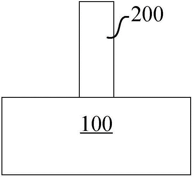
[0021] a. providing a substrate 100, and forming fins 200 on the substrate;

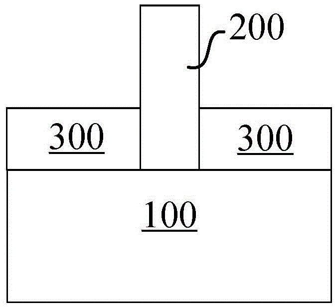
[0022] b. forming isolation layers 300 on the substrates on both sides of the fin 200;

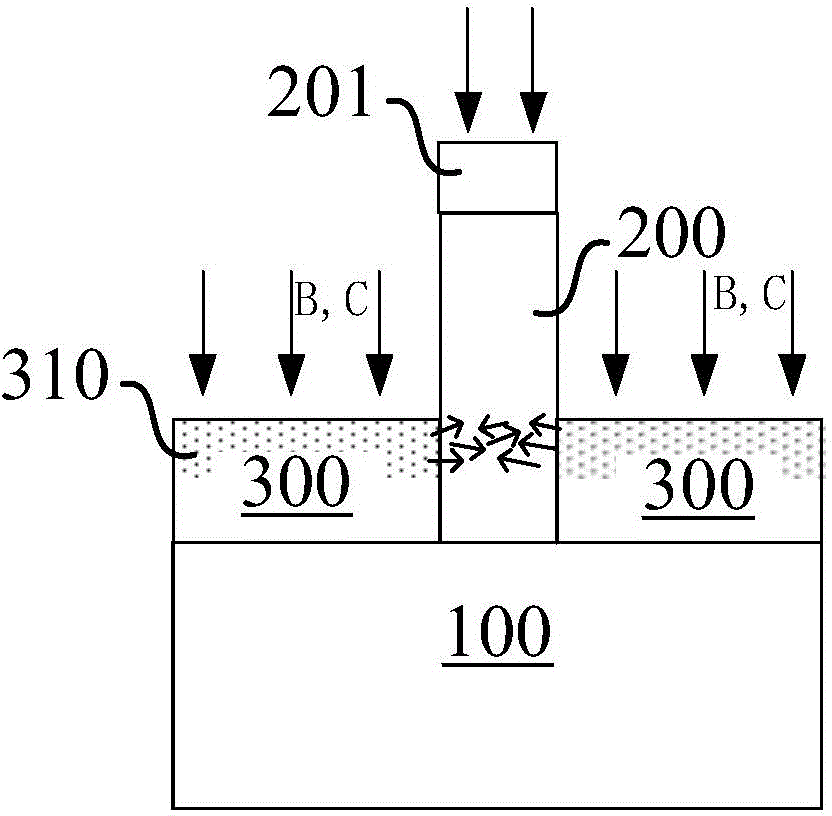
[0023] c. forming a punch-through barrier layer 310 and a diffusion barrier layer 320 in the fins on both sides of the upper half of the isolation layer 300;

[0024] d. Forming source and drain regions at both ends of the fin, forming a gate structure in the middle of the fin, and filling an interlayer dielectric layer 500 above the isolation layer 300 . Wherein, the penetration barrier layer 310 and the diffusion barrier layer 320 are formed by lateral scattering of impurity particles from the isolation layer 300 in...


PUM


Abstract

The invnetion provides a FinFET manufacturing method. The FinFET manufacturing method comprises: a, providing a substrate (100), and forming a fin (200) on the substrate; b, forming isolation layers (300) on the substrate on the two sides of the fin (200); c, forming punchthrough barrier layer (310) and a diffusion barrier layer (320) in the fin on two sides of the upper half parts of the isolation layers (300); and d, forming drain and source regions respectivley at two ends of the fin, forming a gate structure at the middle of the fin, and filling an interlayer medium layer (500) in the upper part of the isolation layers (300). Through the method provided by the invention, PTSL distribution is effectively optimized, and device performance is improved.

Description

technical field [0001] The present invention relates to a method for manufacturing a semiconductor device, in particular to a method for manufacturing a FinFET. technical background [0002] As the size of the semiconductor device is scaled down, there arises a problem that the threshold voltage decreases with the decrease of the channel length, that is, a short channel effect is generated in the semiconductor device. To meet the challenges from semiconductor design and manufacturing, led to the development of Fin Field Effect Transistor, or FinFET. [0003] Channel punch-through effect (Channelpunch-througheffect) is a phenomenon that the source junction and the depletion region of the drain junction of the field effect transistor are connected. When the channel is penetrated, the potential barrier between the source and the drain is significantly reduced, and a large number of carriers are injected from the source to the channel, and drift through the space charge region ...

Claims


Application Information

Patent Timeline
Patent Type & Authority Applications(China)
IPC IPC(8): H01L21/336H01L29/78
CPCH01L29/78H01L29/66803
Inventor 尹海洲刘云飞张珂珂
Owner INST OF MICROELECTRONICS CHINESE ACAD OF SCI
Why Eureka
Try Eureka