Semiconductor device manufacture procedure prediction system and method

A prediction system and prediction method technology, applied in the semiconductor field, can solve the problems of increasing the cost of semiconductor devices, wafer abandonment, etc., and achieve the effect of preventing major reliability and/or yield problems

Inactive Publication Date: 2016-01-06
SEMICON MFG INT (SHANGHAI) CORP
View PDF4 Cites 23 Cited by
  • Summary
  • Abstract
  • Description
  • Claims
  • Application Information

AI Technical Summary

Problems solved by technology

This can lead to high-risk wafers being eventually scrapped due to risk, which in turn increases the cost of the semiconductor device manufacturing process
[0005] It can be seen that there is no solution in the prior art to prevent major reliability or yield problems in the manufacturing process of semiconductor devices through real-time prediction of inline data

Method used


Image

  • Semiconductor device manufacture procedure prediction system and method
  • Semiconductor device manufacture procedure prediction system and method
  • Semiconductor device manufacture procedure prediction system and method

Examples


Embodiment 1

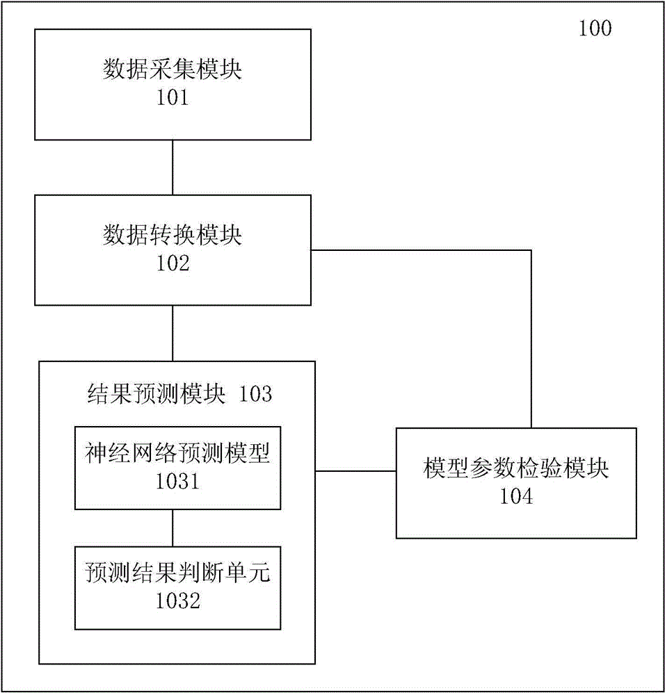
[0057] An embodiment of the present invention provides a semiconductor device manufacturing process prediction system, which can prevent major reliability and / or yield problems in the semiconductor device manufacturing process by collecting online data and predicting the results of the information to be predicted. Among them, the prediction of reliability and / or yield rate results is mainly realized by using a neural network model (NeuralNetworksModule).

[0058] Such as figure 1 As shown, this embodiment provides a semiconductor device manufacturing process prediction system 100 , which includes a data acquisition module 101 , a data conversion module 102 , and a result prediction module 103 . Wherein, the result prediction module 103 includes a neural network prediction unit 1031 and a prediction result judgment unit 1032 . In addition, the semiconductor device process prediction system 100 may further include a prediction unit parameter verification module 104 .

[0059] ...

Embodiment 2

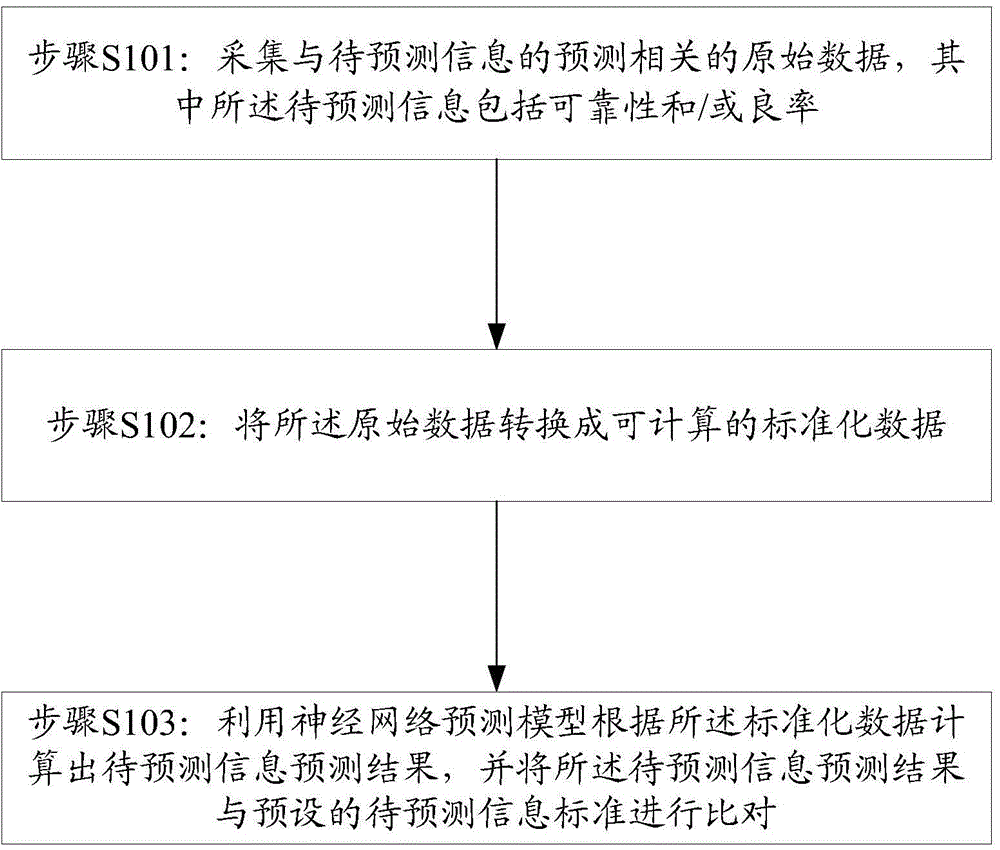
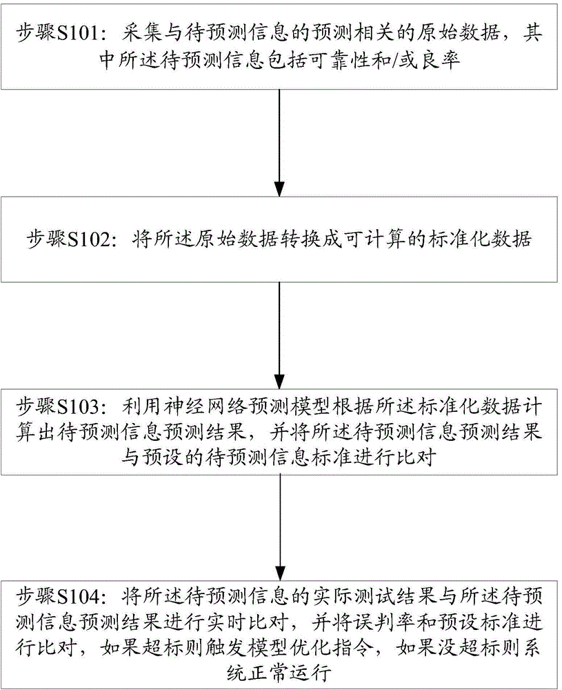
[0112] An embodiment of the present invention provides a semiconductor device manufacturing process prediction method, which is implemented by using the semiconductor device manufacturing process prediction system described in Embodiment 1. The semiconductor device manufacturing process prediction method can prevent major reliability and / or yield rate problems in the semiconductor device manufacturing process by collecting online data and predicting the results of the information to be predicted (reliability or yield rate). Among them, the calculation of the predicted result of the predicted information (such as reliability or yield rate) is mainly realized by using a neural network model.

[0113] Below, refer to figure 2 and image 3 The semiconductor device manufacturing process prediction method of this embodiment will be introduced. in, figure 2 It is a flowchart of a semiconductor device manufacturing process prediction method according to an embodiment of the prese...


PUM


Abstract

The present invention provides a semiconductor device manufacture procedure prediction system and method, and relates to the technical field of semiconductors. The system comprises a data acquisition module, a data conversion module and a result prediction module with a neural network model. The method comprises the steps of collecting prediction-related original data of to-be-predicted information, converting the original data into computable standardized data, and calculating a to-be-predicted information prediction result by using a neural network prediction model. With adoption of the system and the method, the to-be-predicted information prediction result can be timely calculated by using the neural network model according to on-line data, thereby preventing major reliability and / or yield problems occurred in a semiconductor device manufacture procedure.

Description

technical field [0001] The invention relates to the technical field of semiconductors, in particular to a semiconductor device manufacturing process prediction system and method. Background technique [0002] In the field of semiconductor technology, yield and reliability are two important factors affecting the development and profitability of the semiconductor manufacturing industry. Generally, the reliability of a semiconductor device is calculated and obtained according to test results after the manufacturing process of the semiconductor device is completed. Similarly, the yield rate of semiconductor devices can only be obtained from the wafer test results after the process is completed. [0003] Since yield and reliability are very important factors to profitability, how to accurately predict reliability risk and yield is a necessary factor for semiconductor device manufacturers to ensure profitability. [0004] Currently, assessments of reliability risk and yield can ...

Claims


Application Information

Patent Timeline
Patent Type & Authority Applications(China)
IPC IPC(8): H01L21/66
CPCG05B19/41875G05B23/0294G06N3/02G06Q10/0639G06F30/39Y02P90/02
Inventor 简维廷徐孝景康盛
Owner SEMICON MFG INT (SHANGHAI) CORP
Why Eureka
Try Eureka