Machining method of double-face touch screen shadow eliminating conducting glass
A technology of conductive glass and a processing method, which is applied in the processing field of double-sided touch screen erasing conductive glass, can solve problems such as affecting electromagnetic shielding, electrostatic protection function, and viewing pattern effects, and achieves high uniformity, good electromagnetic shielding, and low cost. Effect
- Summary
- Abstract
- Description
- Claims
- Application Information
AI Technical Summary
Problems solved by technology
Method used
Image
Examples
Embodiment 1
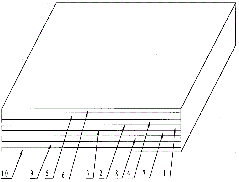
[0027] Both surfaces of the upper glass substrate 1 and the lower glass substrate 7 are the tin surface 2 and the air surface 3, the air surfaces 3 of the upper glass substrate 1 and the lower glass substrate 7 are correspondingly bonded, and the tin surface 2 of the upper glass substrate 1 is set Upper interference layer one 4, upper transparent passivation layer 5 is set between upper interference layer one 4 and upper interference layer two 6, lower interference layer one 8 is set under the tin surface 2 of lower glass substrate 7, lower interference layer one 8 is connected to lower interference layer two A lower transparent passivation layer 9 is arranged between the interference layer 2 10;
[0028] Both the upper transparent passivation layer 5 and the lower transparent passivation layer 9 are made of transparent silicon dioxide or transparent silicon oxynitride;
[0029] The first upper interference layer 4 , the second upper interference layer 6 , the first lower inte...
Embodiment 2
[0031] In the first step, the upper glass substrate 1 and the lower glass substrate 7 are processed,
[0032] A. Cutting the upper glass substrate 1 and the lower glass substrate 7, first X cutting, then Y cutting, and then breaking into pieces;
[0033] B. Perform edging and chamfering on the cut upper glass substrate 1 and lower glass substrate 7, first X edging, then chamfering, rotate 90° and then Y edging and chamfering;
[0034] C. Scrub and dry;
[0035] D, polishing the upper glass substrate 1 and the lower glass substrate 7 after edging and chamfering;
[0036] E, then brush and dry;
[0037] In the second step, the upper interference layer 1 and the lower glass substrate 7 are sputtered with an upper interference layer 4, an upper transparent passivation layer 5, a lower interference layer 8, and a lower transparent passivation layer 9;
[0038] A. After polishing, brushing and drying, the upper glass substrate 1 and the lower glass substrate 7 are bonded together...
PUM
 Abstract
Description
Claims
Application Information
