

High Diffraction Efficiency Mems Scanning Grating with Integrated Angle Sensor
An angle sensor and scanning grating technology, which is applied in the field of MEMS scanning grating to reduce the cost of silicon wafers, improve diffraction efficiency, and achieve the effect of easy
- Summary
- Abstract
- Description
- Claims
- Application Information
AI Technical Summary
Problems solved by technology
Method used
Image

Examples
Embodiment Construction
[0028] The present invention will be described in detail below in conjunction with the accompanying drawings.
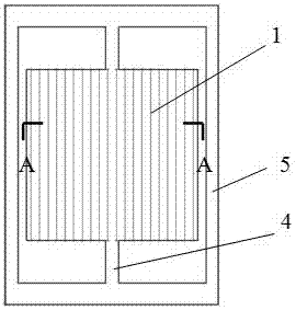
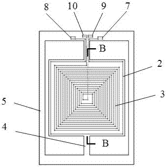
[0029] Referring to FIG. 1 , the high diffraction efficiency MEMS scanning grating integrated with an angle sensor includes a grating surface 1 , an electromagnetic driving coil 2 , an electromagnetic sensing coil 3 , a torsion beam 4 and a supporting frame 5 . The grating surface 1, the electromagnetic driving coil 2, the electromagnetic sensing coil 3, the torsion beam 4 and the supporting frame 5 are all fabricated on the same silicon structure layer 6, and the silicon structure layer 6 is used as the common bottom layer. The grating surface 1 is located on the front side of the silicon structure layer, and the electromagnetic driving coil 2 and the electromagnetic sensing coil 3 are located on the back side of the silicon structure layer. The grating surface 1 , the electromagnetic driving coil 2 and the electromagnetic sensing coil 3 are supported inside the sup...
PUM
 Abstract
Description
Claims
Application Information