A kind of multi-chip side glue removal method

A multi-chip and edge glue technology, which is applied in the direction of equipment, photoplate making process of pattern surface, optics, etc., can solve the problems of wasting chip area and difficult to realize edge washing method, so as to improve production efficiency, avoid chip area waste, The effect of avoiding damage

Active Publication Date: 2019-05-28
SHANGHAI INST OF TECHNICAL PHYSICS - CHINESE ACAD OF SCI
View PDF5 Cites 0 Cited by
  • Summary
  • Abstract
  • Description
  • Claims
  • Application Information

AI Technical Summary

Problems solved by technology

Although the existing edge bead removal process can suppress the sputtering of the photoresist dissolving agent on the inside of the chip and the damage of the wafer to a certain extent through technical improvement (such as Chinese invention patent, CN101819382A), there are still the following problems : 1) At present, all edge removal methods or devices based on solvent edge washing are only suitable for standard-sized wafer chips. For chips with non-standard shapes and sizes, this edge washing method is difficult to achieve; 2) Based on washing The edge glue removal method requires that the processed chip wafer has good mechanical strength (such as Si, GaAs), and can withstand the impact of the solvent liquid and shielding gas sprayed from the nozzle. Therefore, for the mechanical strength of the material For poorer chips (such as CdZnTe, etc.), this edge washing method is also not applicable; 3) In order to avoid the sputtering effect of the photoresist spraying inside the chip, a wider edge of the chip must be left area, which inevitably wastes more chip area for smaller wafers or chips

Method used


Image

  • A kind of multi-chip side glue removal method
  • A kind of multi-chip side glue removal method
  • A kind of multi-chip side glue removal method

Examples


Embodiment Construction

[0017] The specific implementation manner of the present invention will be described below in conjunction with the accompanying drawings.

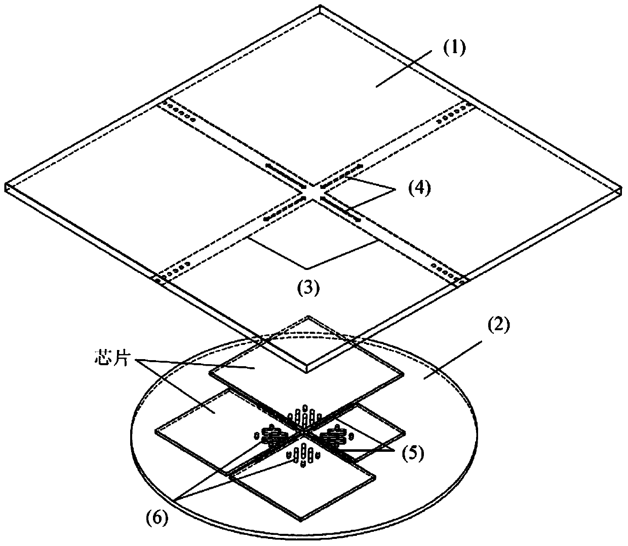
[0018] A method for removing multi-chip edge glue in this embodiment includes a 5-inch photolithography mask (1) for selectively exposing the chip edge glue and a sample suction cup (2) for carrying and positioning chips, the suction cup with a diameter of 4 inches, such as figure 1 shown.

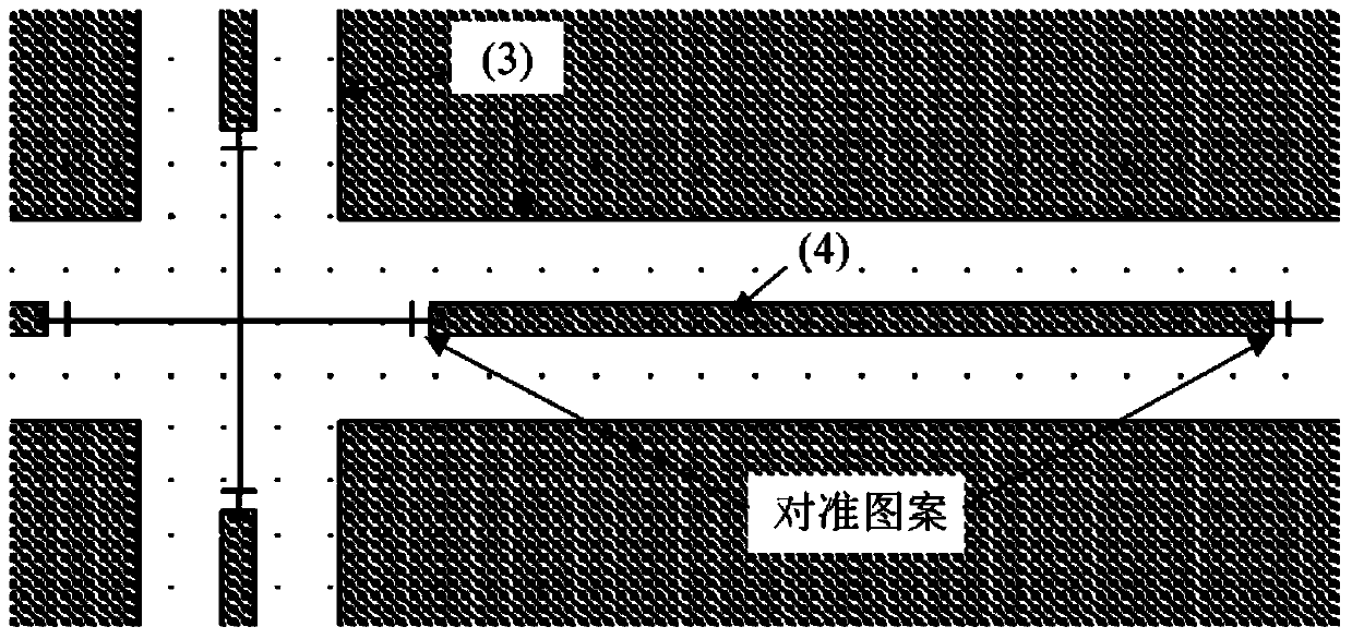
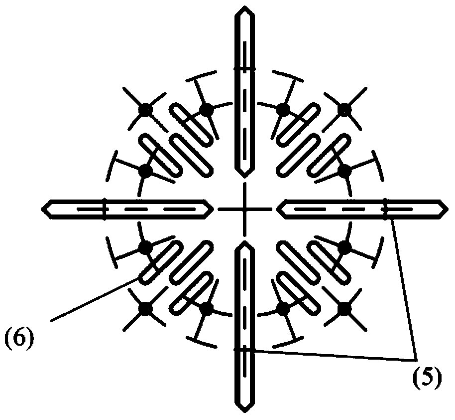
[0019] There is a cross figure (3) covering the whole photoresist plate on the photolithographic mask plate (1). The inside of the cross figure (3) is light-transmissive as a whole, and its outer area is opaque. There are four inside the cross figure (3). A strip-shaped registration mark (4); the registration marks (4) are opaque and arranged in a cross, and the center of symmetry is the center of the cross figure (3); the two ends of each registration mark are aligned pattern, the alignment pattern is a cross, such as figure 2 shown;

[0020] The...


PUM

PropertyMeasurementUnit
diameteraaaaaaaaaa

Abstract

The invention discloses a multi-chip edge glue removal method. A removal device is provided with a photolithography mask and a sample suction cup, wherein the photolithography mask is used for carrying out selective exposure on chip edge glue; the sample suction cup is used for carrying and locating chips; cross bosses on the sample suction cup can be used for locating the chips, and can also be used as registering marks for photolithography; holes are formed in the middle of the sample suction cup and can be matched with the sample suction cup of a photolithography machine to fix the chips; and registering marks corresponding to the cross bosses are arranged in cross patterns on the photolithography mask. Square chips from which the edge glue is to be removed are put on the sample suction cup with the cross locating bosses in the center; two-step exposure is carried out on the chips with the photolithography mask with the registering marks and the cross mask patterns; and after development and fixation, the edge glue of the chips are removed. According to the method, the edge glue removal efficiency on the square chips is improved, so that the extreme dimension and the registration difficulty of a subsequent photolithography process are reduced.

Description

technical field [0001] The invention relates to a photoresist mask edge glue removal technology in a microelectronics process, in particular to a multi-chip photoresist mask edge glue removal method. Background technique [0002] The vigorous development of microelectronics and semiconductor integrated circuit technology has promoted the miniaturization and integration of sensor technology closely related to it. At present, both the detector chip of the micro sensor and the signal processing integrated circuit at the back end are based on the thin film process and photolithography process in microelectronics technology. Therefore, the limit size and lithography precision in the lithography process have become important factors restricting the integration scale and performance of micro sensors and integrated circuit chips. Although electron beam lithography and non-contact exposure technology have become optional technical means to improve the limit size and lithography prec...

Claims


Application Information

Patent Timeline
Patent Type & Authority Patents(China)
IPC IPC(8): G03F7/42G03F9/00H01L21/02
Inventor 施长治林春
Owner SHANGHAI INST OF TECHNICAL PHYSICS - CHINESE ACAD OF SCI
Why Eureka
Try Eureka