

Etching apparatus and etching method
A technology for etching devices and processing space, which is applied in the direction of discharge tubes, electrical components, semiconductor/solid-state device manufacturing, etc., which can solve the problem of etching rate reduction and achieve the effect of increasing etching rate
- Summary
- Abstract
- Description
- Claims
- Application Information
AI Technical Summary
Problems solved by technology
Method used
Image

Examples
no. 1 approach >
[0065]
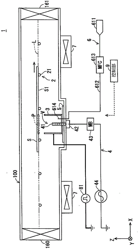
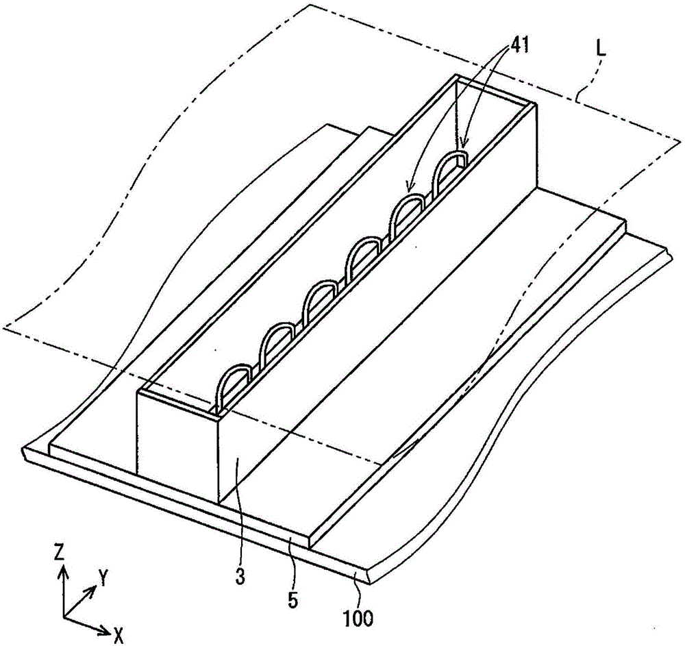
[0066] figure 1 It is a side view schematically showing the schematic structure of the etching apparatus 1 of the first embodiment. figure 2 It is a partial perspective view showing the peripheral portion of the processing space V in the etching apparatus 1 .
[0067] The etching apparatus 1 is an apparatus that generates plasma in a processing space V formed in a chamber 100 and applies processing to one main surface S1 of a substrate S (base material) using the plasma. Hereinafter, a case where an ITO film is formed on the above-mentioned main surface S1 of the substrate S to be processed will be described.
[0068] The etching apparatus 1 mainly includes: a chamber 100; a transport mechanism 2 for transporting a substrate S in the chamber 100; a partition member 3 for defining the range of a processing space V in the chamber 100; a plasma processing unit 4 for Plasma is generated in the processing space V; and the insulating plate 5 is arranged between the upp...
no. 2 approach >
[0099] Figure 4 It is a side view schematically showing a schematic configuration of an etching apparatus 1A according to the second embodiment. Figure 5 It is a partial perspective view showing the peripheral part of the electrode in 1A of etching apparatuses in detail.
[0100] In the following, refer to Figure 4 and Figure 5 The etching apparatus 1A of the second embodiment will be described, however, the same reference numerals will be assigned to the same elements as those of the first embodiment, and repeated description thereof will be omitted. And, to keep the diagram from getting complicated, in the Figure 4 The peripheral part of the electrode is briefly drawn in .
[0101] The etching apparatus 1A differs from the above-mentioned etching apparatus 1 in that the partition member 3A and the electrode 8A are different members. Hereinafter, this point of difference will be mainly described.
[0102] Like the above-mentioned first embodiment, the partition mem...
no. 3 approach >
[0108] Figure 6 It is a side view schematically showing the schematic structure of the etching apparatus 1B of the third embodiment. Figure 7 It is a partial perspective view showing the peripheral part of the electrode in etching apparatus 1B in detail.
[0109] In the following, refer to Figure 6 and Figure 7 The etching apparatus 1B according to the third embodiment will be described, however, the same elements as those in the first embodiment will be assigned the same reference numerals, and repeated description thereof will be omitted. And, to keep the diagram from getting complicated, in the Figure 6 The peripheral part of the electrode is briefly drawn in .
[0110] The electrode 8B in the third embodiment has a substantially L-shape in side view, and has: a first portion 85 covering the upper end of the partition member 3B; and a second portion 86 along the processing space V side of the partition member 3B. wall extension. Therefore, the electrode 8B is dif...
PUM
 Abstract
Description
Claims
Application Information