Sintering fixture for micro channel semiconductor laser and sintering method thereof

A micro-channel and semiconductor technology, applied in the direction of semiconductor lasers, lasers, laser components, etc., can solve the problems of inability to sinter insulating sheets and obtain micro-channel semiconductor laser components, so as to reduce sintering voids, improve reliability and service life , Easy and reliable operation

Inactive Publication Date: 2016-01-13
Shandong Huaguang Optoelectronics Co. Ltd.
View PDF5 Cites 15 Cited by
  • Summary
  • Abstract
  • Description
  • Claims
  • Application Information

AI Technical Summary

Problems solved by technology

The disadvantage of this fixture is that it is designed for sintering the laser chip to the micro-channel heat sink and sintering the negative plate to the chip at the same time, and cannot sinter the insulating sheet necessary for the micro-channel semiconductor laser component to the micro-channel heat sink. Rear part; in addition, since the pressure application part is a fixed plane, the rear part of the negative plate is not fixed on the insulating sheet or the microchannel heat sink after sintering, and is in a suspended state and is not insulated from the main body of the microchannel heat sink. Directly Tested and Assembled Microchannel Diode Laser Components
The disadvantage of this device is that it is aimed at packaging the sintered and well-fixed and electrically connected micro-channel laser components into an assembly and debugging fixture for stacked lasers, which involves the adjustment of positioning accuracy and the assembly of each micro-channel unit. It does not involve the encapsulation and sintering of necessary components such as the microchannel heat sink-laser chip, insulating sheet, negative electrode sheet, etc., and it is impossible to assemble and sinter the microchannel heat sink welded with the laser chip to form a microchannel that can be stacked. Channel Laser Assembly

Method used


Image

  • Sintering fixture for micro channel semiconductor laser and sintering method thereof
  • Sintering fixture for micro channel semiconductor laser and sintering method thereof
  • Sintering fixture for micro channel semiconductor laser and sintering method thereof

Examples


Embodiment Construction

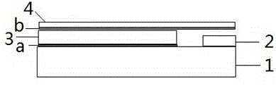
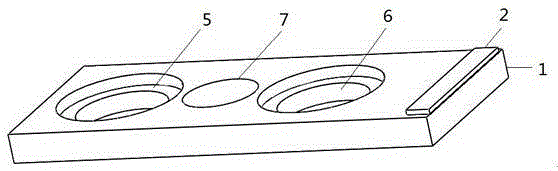
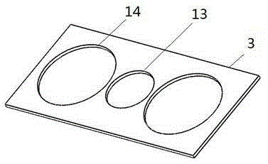
[0038] The sintering fixture of the microchannel semiconductor laser of the present invention is used for figure 1 The sintering of the micro-channel bar laser is shown, the micro-channel bar laser is that the laser bar chip 2 is arranged on the micro-channel heat sink 1, and the insulating sheet 3 is sintered on the micro-channel heat sink 1 through the insulating solder layer a, A negative electrode sheet 4 is sintered on the insulating sheet 3 through the negative electrode solder layer b. Wherein the structure of the microchannel heat sink 1 is as follows figure 2As shown, a sealing groove 5, a water hole 6 and a positioning hole 7 are arranged on it, and the laser bar chip 2 is arranged on one side of the microchannel heat sink 1. The structure of insulating sheet 3 is as image 3 As shown, a lower positioning and fixing hole 13 and a lower water passage opening 14 are arranged on it. The structure of the negative plate is as Figure 4 As shown, upper positioning and...


PUM


Abstract

The invention discloses a sintering fixture for a micro channel semiconductor laser and a sintering method thereof. The sintering fixture comprises a positioning base and an adjustable cover plate, wherein the adjustable cover plate is connected onto the positioning base; a concave surface is arranged on the positioning base; two sides of the concave surface are bosses; the adjustable cover plate comprises a main body, a pressing block and a pressing block adjustment mechanism, the main body is provided with a pressing block groove, and the pressing block is arranged inside the pressing block groove via the pressing block adjustment mechanism. The micro channel semiconductor laser sintering method by the above device comprises steps: a micro channel heat sink sintered with a semiconductor laser bar chip, an insulated sheet and the adjustable cover plate are sequentially connected onto the positioning base from bottom to top and fixed by using bolts, and the above well-fixed entire fixture is sealed in a protection cover shell with nitrogen and is placed on a heating table for sintering. According to the sintering fixture for the micro-channel semiconductor laser and the sintering method thereof, the structure is simple, the cost is low, the operation is simple, convenient and reliable, and through one-time sintering, quick and accurate fixed connection among the bar chip of the micro-channel semiconductor laser, the micro-channel heat sink, the insulated sheet and a negative electrode sheet can be realized.

Description

technical field [0001] The invention relates to a jig for encapsulating micro-channel semiconductor laser components used in the manufacture of high-power lasers, and a sintering method for the micro-channel semiconductor laser by the jig, belonging to the technical field of semiconductor laser sintering. Background technique [0002] In recent years, due to the unique characteristics of small size, light weight, high efficiency and reliability of semiconductor lasers, the use of high-power semiconductor lasers has gradually expanded, and has been used in solid-state laser pumping, medical treatment, display lighting, laser processing and military fields. more and more widely used. With the gradual optimization of the chip structure of high-power semiconductor lasers and the advancement of packaging technology, the preparation and application of laser bar chip arrays with output powers above kilowatts are also increasing rapidly. The use of laser bar chip arrays can greatly...

Claims


Application Information

Patent Timeline
Patent Type & Authority Applications(China)
IPC IPC(8): H01S5/022H01S5/024
Inventor 杨扬孙素娟李沛旭徐现刚
Owner Shandong Huaguang Optoelectronics Co. Ltd.
Why Eureka
Try Eureka