

Silicon carbide semiconductor device and method for manufacturing same
An oxide semiconductor, semiconductor technology, applied in semiconductor/solid-state device manufacturing, semiconductor devices, electrical components, etc., can solve problems such as self-conduction and threshold voltage reduction
- Summary
- Abstract
- Description
- Claims
- Application Information
AI Technical Summary
Problems solved by technology
Method used
Image

Examples
no. 1 approach
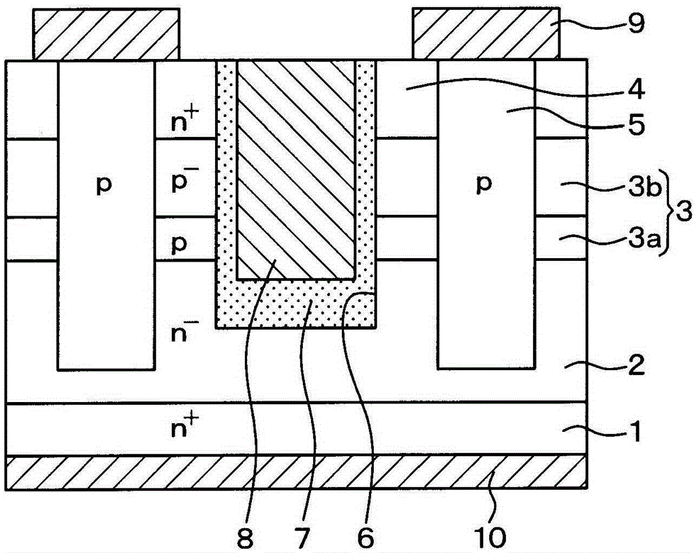
[0028] refer to figure 1 A SiC semiconductor device in which an inverted vertical MOSFET with a trench gate structure is formed according to the first embodiment of the present application will be described.
[0029] figure 1 The shown SiC semiconductor device has a structure in which a vertical MOSFET with a trench gate structure is formed in a cell region, and although not shown, has a peripheral withstand voltage structure in an outer peripheral region surrounding the cell region.
[0030] SiC semiconductor devices use n + The front side of type substrate 1 is formed by the n + type substrate 1 compared to SiC with low impurity concentration n - A semiconductor substrate made of a type drift layer 2 is formed. no + type substrate 1 is set, for example, to have an n-type impurity concentration of 1.0×10 19 / cm 3 , n - type drift layer 2 is set, for example, to have an n-type impurity concentration of 0.5 to 2.0×10 16 / cm 3 .
[0031] in n - Base region 3 is forme...
no. 2 approach
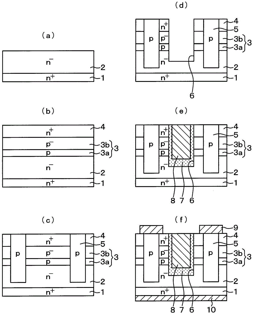
[0059] A second embodiment of the present application will be described. Compared with the first embodiment, this embodiment has changed p + The rest of the structure of the SiC layer 5 is the same as that of the first embodiment, so only the parts different from the first embodiment will be described.
[0060] Such as Figure 5 As shown, in this embodiment, compared with the first embodiment, p + type SiC layer 5 depth such that p + Type SiC layer 5 has a depth up to a position in contact with base region 3 . with p + The various effects described in the first embodiment can also be obtained in the SiC layer 5 . Furthermore, since p + Type SiC layer 5 can be formed deep, so it is possible to pass from n + Type source region 4 surface ion implantation of p-type impurities to form p + Type SiC layer 5. Therefore, unlike the first embodiment, by embedding p in the trench + p + Compared with the case of the SiC layer 5, the manufacturing process can be simplified by ad...
no. 3 approach
[0063] A third embodiment of the present application will be described. This embodiment also changes p from the first embodiment + The rest of the structure of the SiC layer 5 is the same as that of the first embodiment, so only the parts different from the first embodiment will be described.
[0064] Such as Image 6 As shown, in this embodiment, p + Type SiC layer 5 is formed by dividing into two in the depth direction. Specifically, let it be assumed to have from n - The surface of the type drift layer 2 is formed to the lower layer portion 5a deeper than the trench gate structure, and from n + The structure of the upper layer portion 5b formed in such a way that the surface of the type source region 4 reaches the base region 3 . Played by the lower part 5a as p + The role of the deep layer is played by the upper part 5b as p + The role of the type contact layer.
[0065] with p + The various effects described in the first embodiment can also be obtained in the SiC...
PUM
| Property | Measurement | Unit |
|---|---|---|
| Thickness | aaaaa | aaaaa |
| Thickness | aaaaa | aaaaa |
Abstract
Description
Claims
Application Information