
Method for producing silica microlens

A technology of silicon dioxide and manufacturing method, which is applied in lenses, optics, instruments, etc., and can solve the problems of lens surface distortion, complex process, and unsuitable for mass production.

Active Publication Date: 2017-01-11
HENAN SHIJIA PHOTONS TECH
View PDF7 Cites 0 Cited by
  • Summary
  • Abstract
  • Description
  • Claims
  • Application Information

AI Technical Summary

Problems solved by technology

[0008] The invention aims to solve technical problems such as lens surface distortion, background noise, complex process, high cost, difficulty in ensuring product consistency, and unsuitability for large-scale mass production in the existing microlens and microlens array manufacturing technology. Provide a microlens compatible with semiconductor technology, easy to integrate, small in size, low in cost, customizable, suitable for mass production, and a manufacturing method thereof

Method used


Image

  • Method for producing silica microlens
  • Method for producing silica microlens
  • Method for producing silica microlens

Examples


Embodiment Construction

[0053] In this embodiment, N=3 is taken as an example for illustration.

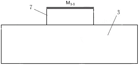
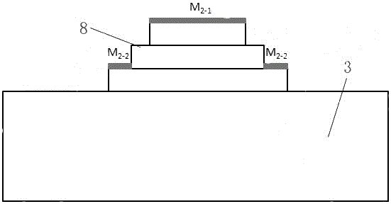
[0054] Such as Figure 1-8 Shown, a kind of manufacture method of silica microlens, the steps are as follows:

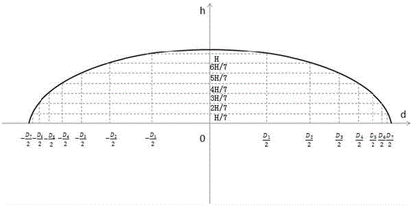
[0055] Step S1: Determine the lens height H of the microlens and the number of photolithography N, then the lens height of the microlens is equally divided into 2 N -1 copy.

[0056] Wherein, the number of times of photolithography N=3, then the lens height of the microlens is equally divided into 2 N -1 = 7 copies.

[0057] Step S2: According to the distance between the horizontal line of the lens height H at each equal height and the two intersection points of the microlens surface characteristic function, determine the cylinder diameters at the corresponding heights in the coaxial cylinder stack structure, respectively D 1 、D 2 、D 3 、D 4 、D 5 、D 6 and D 7 .

[0058] Step S3: According to the calculation result in step S2, calculate the mask layer M to be formed before the N-n phot...


PUM


Abstract

The invention discloses a method for manufacturing a silicon dioxide microlens. Firstly, the lens height and the photoetching frequency are determined; according to a distance between two intersection points of a horizontal line at each equally-divided height section of the lens height H and a microlens surface characteristic function, a cylinder diameter at the corresponding height in a coaxial cylinder stacked structure is determined; the depth of each lens etching is determined; and using a binary optics technology, a 2N-level stepped structure is formed through N-times register photoetching. The photoetching frequency is low, the lens surface form which is practically manufactured can be well meet theoretical design requirements, and processing controllability of the lens surface form is achieved.

Description

technical field [0001] The invention belongs to the technical field of optical devices, and in particular relates to a method for manufacturing a silicon dioxide microlens. Background technique [0002] A lens is a passive optical element used in an optical system to converge and diverge light radiation. Lenses manufactured by traditional techniques are not only complicated in manufacturing method, but also large in size and heavy in weight, which can no longer meet the needs of today's technological development. At present, people have been able to produce lenses with very small diameters, which can only be observed with equipment such as microscopes, scanning electron microscopes, and atomic force microscopes. This is a microlens. Microlenses and microlens arrays have broad application prospects in the fields of optical communication, optical sensing, and optical computing due to their advantages of small size, light weight, easy integration, and array formation. [0003...

Claims


Application Information

Patent Timeline
Patent Type & Authority Patents(China)
IPC IPC(8): G02B3/00
CPCG02B3/0006G02B3/0012
Inventor 田亮安俊明尹小杰张家顺
Owner HENAN SHIJIA PHOTONS TECH
Learn More