High-conversion-efficiency potential-induced degradation (PID)-resisting crystalline silicon solar cell and manufacturing method thereof

A solar cell, conversion efficiency technology, applied in the direction of final product manufacturing, sustainable manufacturing/processing, circuits, etc., can solve the problems of high production cost of anti-PID crystalline silicon solar cells, low cell conversion efficiency, etc., to reduce migration, High cell conversion efficiency and reduced ion accumulation

Inactive Publication Date: 2016-01-27
TRINA SOLAR CO LTD
View PDF5 Cites 7 Cited by
  • Summary
  • Abstract
  • Description
  • Claims
  • Application Information

AI Technical Summary

Problems solved by technology

[0003] The present invention aims at the technical problems of high production cost and low conversion efficiency of anti-PID crystalline silicon solar cells in the prior art, and provides a high conversion efficiency anti-PID crystalline silicon solar cell and its manufacturing method

Method used


Image

  • High-conversion-efficiency potential-induced degradation (PID)-resisting crystalline silicon solar cell and manufacturing method thereof

Examples


Embodiment Construction

[0018] The structure of the present invention will be described in further detail below in conjunction with the accompanying drawings and specific embodiments, and the parts in the present invention that are the same as those of the prior art will be referred to the prior art.

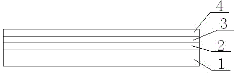
[0019] like figure 1 As shown, the high conversion efficiency anti-PID crystalline silicon solar cell of the present invention includes a silicon wafer 1, a high refractive index silicon nitride passivation layer 2 deposited on the front side of the silicon wafer, with a refractive index of 2.2~2.3 and a film thickness of 1~2. 10nm; the graphene conductive layer 3 coated on the high refractive index silicon nitride passivation layer 2, with a thickness of 1~10nm; the refractive index silicon nitride anti-reflection layer 4 deposited on the graphene conductive layer 3, the refractive index It is 2.0~2.1, and the film thickness is 60~80nm.

[0020] The manufacturing method of high conversion efficiency ...


PUM

PropertyMeasurementUnit
thicknessaaaaaaaaaa
thicknessaaaaaaaaaa
refractive indexaaaaaaaaaa

Abstract

The present invention discloses a high-conversion-efficiency potential-induced degradation (PID)-resisting crystalline silicon solar cell. The solar cell comprises a silicon wafer, and is characterized in that a high refractive index silicon nitride passivation layer, a grapheme conducting layer and a low refractive index silicon nitride passivation layer, which are arranged in turn on a front face of the silicon wafer. Meanwhile, a manufacturing method of the above solar cell is also provided, and comprises the steps of selecting the silicon wafer and carrying out texturization, diffusion and post cleaning; depositing the high refractive index silicon nitride passivation layer on the front face of the silicon wafer, the refractive index being 2.2-2.3 and the film thickness being 1-10 nm; spin coating a grapheme dispersion liquid on the silicon nitride, and then carrying out follow-up drying to form the grapheme conducting layer, the thickness being 1-10 nm; depositing the low refractive index silicon nitride passivation layer on the grapheme conducting layer, the refractive index being 2.0-2.1 and the film thickness being 60-80 nm; and completing back electrode, back electric field and positive electrode printing, drying and sintering, thus to form the cell. The crystalline silicon solar cell provided by the present invention has excellent PID-resisting performance and high battery conversion efficiency.

Description

technical field [0001] The invention relates to an anti-PID solar cell, in particular to an anti-PID crystalline silicon solar cell with high conversion efficiency and a manufacturing method thereof. Background technique [0002] As early as 2005, Sunpower discovered that the PID (potential-induced degradation) phenomenon existed in crystalline silicon back-contact N-type cells after positive high voltage was applied to the module, and more and more attention was paid to the PID of crystalline silicon cells in the future. . As the PID phenomenon is known by more people, more research institutes have studied it. The study found the occurrence of PID phenomenon in p-type crystalline silicon and Na in glass + It is related to the migration from glass to battery under the action of external electric field. In order to slow down the occurrence of PID attenuation, the main way is to prevent Na ions from migrating into the silicon chip. The methods are: a. By increasing the resi...

Claims


Application Information

Patent Timeline
Patent Type & Authority Applications(China)
IPC IPC(8): H01L31/068H01L31/0216H01L31/18
CPCY02E10/547Y02P70/50
Inventor 王子港陈奕峰崔艳峰
Owner TRINA SOLAR CO LTD
Why Eureka
Try Eureka