Preparation method of large-area perovskite micro-nano wire array and application thereof

A perovskite, micro-nano technology, applied in nanotechnology, semiconductor/solid-state device manufacturing, photovoltaic power generation, etc., can solve problems such as difficulty in forming organic lead halide perovskite nanowire array array devices

Active Publication Date: 2016-01-27
湖南纳昇电子科技有限公司
View PDF4 Cites 21 Cited by
  • Summary
  • Abstract
  • Description
  • Claims
  • Application Information

AI Technical Summary

Problems solved by technology

Although there are related nanowire reports (NanoLett., 2014, 14, 6761), the prepared organic lead halide perovskites are all small-area disordered nanowires, and it is difficult to form large-area organic lead halide perovskites. Mineral nanowire array and array device

Method used


Image

  • Preparation method of large-area perovskite micro-nano wire array and application thereof
  • Preparation method of large-area perovskite micro-nano wire array and application thereof
  • Preparation method of large-area perovskite micro-nano wire array and application thereof

Examples


Embodiment 1

[0024] Dissolve 16mg of CH3NH3I in 1ml of DMF, and stir for 2min with a magnet; put 46mg of PbI2 into the prepared DMF solution of CH3NH3I, and stir at a constant temperature on a hot stage at 40°C for 2h to obtain a perovskite CH3NH3PbI3 precursor solution.

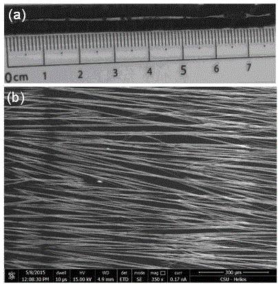
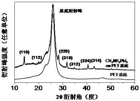
[0025] Take a PET substrate of A4 size (210mm×297mm) or a SiO2 substrate of 50mm×100mm, wipe it with a dust-free cloth dipped in alcohol, dry it with a hair dryer, and then treat it with ozone for 15 minutes; drop the prepared perovskite CH3NH3PbI3 precursor solution on the substrate Apply in a straight line, then scrape the solution with a scraper at a speed of 1m / min to form a uniform film, and let it dry at room temperature; anneal the film formed by scraping at 80°C for 20 minutes to form perovskite CH3NH3PbI3 micronanowire arrays. as attached Figure 1 The CH3NH3PbI3 micro-nanowire array formed by scraping coating on the ET substrate is shown, and Figure II The XRD results prove that the CH3NH3PbI3 crystals of mi...

Embodiment 2

[0028] Dissolve 150mg of CH3NH3I in 15ml of DMF, and stir for 2 minutes with a magnet; put 441mg of PbI2 into the DMF solution of CH3NH3I prepared, and stir for 1.5 hours at a constant temperature on a hot stage at 60°C to obtain a perovskite CH3NH3PbI3 precursor solution.

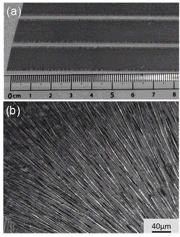
[0029] Referring to our previous roll-to-roll printing equipment invention patent (CN201420230074.X), the perovskite CH3NH3PbI3 solution was prepared by roll-to-roll microgravure printing. The width of the flexible PET substrate is 15cm, and the substrate speed is 0.5m / min. Printing preparation can form a uniform perovskite CH3NH3I film. After passing through a 70°C oven, it can self-assemble to form a CH3NH3PbI3 micro-nano wire array film, such as Figure four shown.

[0030] On the CH3NH3PbI3 micro-nano wire array prepared above, a mask plate with a channel length of 80 μm and a channel width of 1000 μm was used to cover the CH3NH3PbI3 micro-nano wire array film, and a layer of about 40 nm thick gold ele...

Embodiment 3

[0032] Dissolve 150mg of CH3NH3I in 15ml of DMF, and stir for 2 minutes with a magnet; put 262mg of PbCl2 into the prepared DMF solution of CH3NH3I, and stir at a constant temperature on a hot stage at 60°C for 2 hours to obtain a perovskite CH3NH3PbIxCl3-x precursor solution.

[0033] Referring to our previous roll-to-roll printing equipment invention patent (CN201420230074.X), the perovskite CH3NH3PbIxCl3-x solution was prepared by roll-to-roll slit coating printing. Printing preparation at a substrate speed can form a uniform perovskite CH3NH3PbIxCl3-x film. After passing through a 70°C oven, it can self-assemble to form a CH3NH3PbIxCl3-x micro-nano wire array film.


PUM


Abstract

The invention discloses a preparation method of a large-area perovskite micro-nano wire array and an application thereof in a photoelectric detector. Under environment conditions, a highly-oriented large-area micro-nano wire array can be obtained by a simple knife coating mode or a roll-to-roll printing technology. The length of an obtained micro-nano wire reaches the millimeter level, the width is in the range from 100 nanometers to 5 micrometers, and the micro-nano wire array is arranged in a highly-oriented manner. The preparation method is simple, the cost is low, and the highly-oriented large-area micro-nano wire array can be used for preparing the photoelectric detector.

Description

technical field [0001] The invention relates to a preparation method and application of a large-area perovskite micro-nano wire array, and belongs to the technical field of organic-inorganic hybrid nanomaterial preparation. Background technique [0002] In recent years, based on organic-inorganic hybrid organic lead halide perovskite materials have been applied to solar cells, a breakthrough has been achieved, and the photoelectric conversion efficiency has increased from the initial 3% to about 20% (J.Am.Chem.Soc Nature, 2009, 131, 6050; Nature, 2013, 499, 316; Nature, 2013, 501, 395; Nature, 2014, 345, 542; Science, 2014, 344, 458). Organic lead halide perovskite materials have the advantages of good optical properties, high mobility, long carrier diffusion distance, low price, and printing preparation, and have become the most promising new solar cell materials. Moreover, organic lead halide perovskite materials can be applied to the preparation of optoelectronic functio...

Claims


Application Information

Patent Timeline
Patent Type & Authority Applications(China)
IPC IPC(8): H01L51/42H01L51/46H01L51/48H01L31/09B82Y40/00
CPCH01L31/09B82Y40/00H10K30/00Y02E10/549
Inventor 阳军亮胡巧吴涵
Owner 湖南纳昇电子科技有限公司
Why Eureka
Try Eureka